Home > Press > University of Kentucky physicist discovers new 2-D material that could upstage graphene
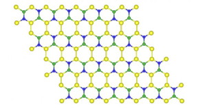 |
| The atoms in the new structure are arranged in a hexagonal pattern as in graphene, but that is where the similarity ends. The three elements forming the new material all have different sizes; the bonds connecting the atoms are also different. As a result, the sides of the hexagons formed by these atoms are unequal, unlike in graphene. CREDIT: Madhu Menon |
Abstract:
A new one atom-thick flat material that could upstage the wonder material graphene and advance digital technology has been discovered by a physicist at the University of Kentucky working in collaboration with scientists from Daimler in Germany and the Institute for Electronic Structure and Laser (IESL) in Greece.
University of Kentucky physicist discovers new 2-D material that could upstage graphene
lexington, KY | Posted on March 4th, 2016Reported in Physical Review B, Rapid Communication, the new material is made up of silicon, boron and nitrogen - all light, inexpensive and earth abundant elements - and is extremely stable, a property many other graphene alternatives lack.
"We used simulations to see if the bonds would break or disintegrate - it didn't happen," said Madhu Menon, a physicist in the UK Center for Computational Sciences. "We heated the material up to 1,000 degree Celsius and it still didn't break."
Using state-of-the-art theoretical computations, Menon and his collaborators Ernst Richter from Daimler and a former UK Department of Physics and Astronomy post-doctoral research associate, and Antonis Andriotis from IESL, have demonstrated that by combining the three elements, it is possible to obtain a one atom-thick, truly 2D material with properties that can be fine-tuned to suit various applications beyond what is possible with graphene.
While graphene is touted as being the world's strongest material with many unique properties, it has one downside: it isn't a semiconductor and therefore disappoints in the digital technology industry. Subsequent search for new 2D semiconducting materials led researchers to a new class of three-layer materials called transition-metal dichalcogenides (TMDCs). TMDCs are mostly semiconductors and can be made into digital processors with greater efficiency than anything possible with silicon. However, these are much bulkier than graphene and made of materials that are not necessarily earth abundant and inexpensive.
Searching for a better option that is light, earth abundant, inexpensive and a semiconductor, the team led by Menon studied different combinations of elements from the first and second row of the Periodic Table.
Although there are many ways to combine silicon, boron and nitrogen to form planar structures, only one specific arrangement of these elements resulted in a stable structure. The atoms in the new structure are arranged in a hexagonal pattern as in graphene, but that is where the similarity ends.
The three elements forming the new material all have different sizes; the bonds connecting the atoms are also different. As a result, the sides of the hexagons formed by these atoms are unequal, unlike in graphene. The new material is metallic, but can be made semiconducting easily by attaching other elements on top of the silicon atoms.
The presence of silicon also offers the exciting possibility of seamless integration with the current silicon-based technology, allowing the industry to slowly move away from silicon instead of eliminating it completely, all at once.
"We know that silicon-based technology is reaching its limit because we are putting more and more components together and making electronic processors more and more compact," Menon said. "But we know that this cannot go on indefinitely; we need smarter materials."
Furthermore, in addition to creating an electronic band gap, attachment of other elements can also be used to selectively change the band gap values - a key advantage over graphene for solar energy conversion and electronics applications.
Other graphene-like materials have been proposed but lack the strengths of the material discovered by Menon and his team. Silicene, for example, does not have a flat surface and eventually forms a 3D surface. Other materials are highly unstable, some only for a few hours at most.
The bulk of the theoretical calculations required were performed on the computers at the UK Center for Computational Sciences with collaborators Richter and Andriotis directly accessing them through fast networks. Now the team is working in close collaboration with a team led by Mahendra Sunkara of the Conn Center for Renewable Energy Research at University of Louisville to create the material in the lab. The Conn Center team has had close collaborations with Menon on a number of new materials systems where they were able to test his theory with experiments for a number of several new solar materials.
"We are very anxious for this to be made in the lab," Menon said. "The ultimate test of any theory is experimental verification, so the sooner the better!"
Some of the properties, such as the ability to form various types of nanotubes, are discussed in the paper but Menon expects more to emerge with further study.
"This discovery opens a new chapter in material science by offering new opportunities for researchers to explore functional flexibility and new properties for new applications," he said. "We can expect some surprises."
####
About University of Kentucky
UK is the University for Kentucky. At UK, we are educating more students, treating more patients with complex illnesses and conducting more research and service than at any time in our 150-year history. To read more about the UK story and how you can support continued investment in your university and the Commonwealth, go to: uky.edu/uk4ky. #uky4ky #seeblue
For more information, please click here
Contacts:
Whitney Harder
859-323-2396
Copyright © University of Kentucky
If you have a comment, please Contact us.Issuers of news releases, not 7th Wave, Inc. or Nanotechnology Now, are solely responsible for the accuracy of the content.
Bookmark:


| Related News Press |
News and information
![]() Quantum computer improves AI predictions April 17th, 2026
Quantum computer improves AI predictions April 17th, 2026
![]() Flexible sensor gains sensitivity under pressure April 17th, 2026
Flexible sensor gains sensitivity under pressure April 17th, 2026
![]() A reusable chip for particulate matter sensing April 17th, 2026
A reusable chip for particulate matter sensing April 17th, 2026
![]() Detecting vibrational quantum beating in the predissociation dynamics of SF6 using time-resolved photoelectron spectroscopy April 17th, 2026
Detecting vibrational quantum beating in the predissociation dynamics of SF6 using time-resolved photoelectron spectroscopy April 17th, 2026
Graphene/ Graphite
![]() Electrifying results shed light on graphene foam as a potential material for lab grown cartilage June 6th, 2025
Electrifying results shed light on graphene foam as a potential material for lab grown cartilage June 6th, 2025
![]() Breakthrough in proton barrier films using pore-free graphene oxide: Kumamoto University researchers achieve new milestone in advanced coating technologies September 13th, 2024
Breakthrough in proton barrier films using pore-free graphene oxide: Kumamoto University researchers achieve new milestone in advanced coating technologies September 13th, 2024
Discoveries
![]() Quantum computer improves AI predictions April 17th, 2026
Quantum computer improves AI predictions April 17th, 2026
![]() Flexible sensor gains sensitivity under pressure April 17th, 2026
Flexible sensor gains sensitivity under pressure April 17th, 2026
![]() A reusable chip for particulate matter sensing April 17th, 2026
A reusable chip for particulate matter sensing April 17th, 2026
![]() Detecting vibrational quantum beating in the predissociation dynamics of SF6 using time-resolved photoelectron spectroscopy April 17th, 2026
Detecting vibrational quantum beating in the predissociation dynamics of SF6 using time-resolved photoelectron spectroscopy April 17th, 2026
Materials/Metamaterials/Magnetoresistance
![]() First real-time observation of two-dimensional melting process: Researchers at Mainz University unveil new insights into magnetic vortex structures August 8th, 2025
First real-time observation of two-dimensional melting process: Researchers at Mainz University unveil new insights into magnetic vortex structures August 8th, 2025
![]() Researchers unveil a groundbreaking clay-based solution to capture carbon dioxide and combat climate change June 6th, 2025
Researchers unveil a groundbreaking clay-based solution to capture carbon dioxide and combat climate change June 6th, 2025
![]() A 1960s idea inspires NBI researchers to study hitherto inaccessible quantum states June 6th, 2025
A 1960s idea inspires NBI researchers to study hitherto inaccessible quantum states June 6th, 2025
![]() Institute for Nanoscience hosts annual proposal planning meeting May 16th, 2025
Institute for Nanoscience hosts annual proposal planning meeting May 16th, 2025
Announcements
![]() A fundamentally new therapeutic approach to cystic fibrosis: Nanobody repairs cellular defect April 17th, 2026
A fundamentally new therapeutic approach to cystic fibrosis: Nanobody repairs cellular defect April 17th, 2026
![]() UC Irvine physicists discover method to reverse �quantum scrambling� : The work addresses the problem of information loss in quantum computing system April 17th, 2026
UC Irvine physicists discover method to reverse �quantum scrambling� : The work addresses the problem of information loss in quantum computing system April 17th, 2026
Interviews/Book Reviews/Essays/Reports/Podcasts/Journals/White papers/Posters
![]() A fundamentally new therapeutic approach to cystic fibrosis: Nanobody repairs cellular defect April 17th, 2026
A fundamentally new therapeutic approach to cystic fibrosis: Nanobody repairs cellular defect April 17th, 2026
![]() UC Irvine physicists discover method to reverse �quantum scrambling� : The work addresses the problem of information loss in quantum computing system April 17th, 2026
UC Irvine physicists discover method to reverse �quantum scrambling� : The work addresses the problem of information loss in quantum computing system April 17th, 2026
Research partnerships
![]() Lab to industry: InSe wafer-scale breakthrough for future electronics August 8th, 2025
Lab to industry: InSe wafer-scale breakthrough for future electronics August 8th, 2025
![]() HKU physicists uncover hidden order in the quantum world through deconfined quantum critical points April 25th, 2025
HKU physicists uncover hidden order in the quantum world through deconfined quantum critical points April 25th, 2025
|
|
||
|
|
||
| The latest news from around the world, FREE | ||
|
|
||
|
|
||
| Premium Products | ||
|
|
||
|
Only the news you want to read!
Learn More |
||
|
|
||
|
Full-service, expert consulting
Learn More |
||
|
|
||