Home > Press > Silicon chip with integrated laser: Light from a nanowire: Nanolaser for information technology
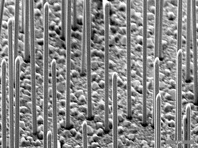 |
| Gallium-arsenide nanowires are on a silicon surface. CREDIT: Thomas Stettner/Philipp Zimmermann / TUM |
Abstract:
Physicists at the Technical University of Munich (TUM) have developed a nanolaser, a thousand times thinner than a human hair. Thanks to an ingenious process, the nanowire lasers grow right on a silicon chip, making it possible to produce high-performance photonic components cost-effectively. This will pave the way for fast and efficient data processing with light in the future.
Silicon chip with integrated laser: Light from a nanowire: Nanolaser for information technology
Munich, Germany | Posted on February 12th, 2016Ever smaller, ever faster, ever cheaper - since the start of the computer age the performance of processors has doubled on average every 18 months. 50 years ago already, Intel co-founder Gordon E. Moore prognosticated this astonishing growth in performance. And Moore's law seems to hold true to this day.
But the miniaturization of electronics is now reaching its physical limits. "Today already, transistors are merely a few nanometers in size. Further reductions are horrendously expensive," says Professor Jonathan Finley, Director of the Walter Schottky Institute at TUM. "Improving performance is achievable only by replacing electrons with photons, i.e. particles of light."
Photonics - the silver bullet of miniaturization
Data transmission and processing with light has the potential of breaking the barriers of current electronics. In fact, the first silicon-based photonics chips already exist. However, the sources of light for the transmission of data must be attached to the silicon in complicated and elaborate manufacturing processes. Researchers around the world are thus searching for alternative approaches.
Scientists at the TU Munich have now succeeded in this endeavor: Dr. Gregor Koblm�ller at the Department of Semiconductor Quantum-Nanosystems has, in collaboration with Jonathan Finley, developed a process to deposit nanolasers directly onto silicon chips. A patent for the technology is pending.
Growing a III-V semiconductor onto silicon requires tenacious experimentation. "The two materials have different lattice parameters and different coefficients of thermal expansion. This leads to strain," explains Koblm�ller. "For example, conventional planar growth of gallium arsenide onto a silicon surface results therefore in a large number of defects."
The TUM team solved this problem in an ingenious way: By depositing nanowires that are freestanding on silicon their footprints are merely a few square nanometers. The scientists could thus preclude the emerging of defects in the GaAs material.
Atom by atom to a nanowire
But how do you turn a nanowire into a vertical-cavity laser? To generate coherent light, photons must be reflected at the top and bottom ends of the wire, thereby amplifying the light until it reaches the desired threshold for lasing.
To fulfil these conditions, the researchers had to develop a simple, yet sophisticated solution: "The interface between gallium arsenide and silicon does not reflect light sufficiently. We thus built in an additional mirror - a 200 nanometer thick silicon oxide layer that we evaporated onto the silicon," explains Benedikt Mayer, doctoral candidate in the team led by Koblm�ller and Finley. "Tiny holes can then be etched into the mirror layer. Using epitaxy, the semiconductor nanowires can then be grown atom for atom out of these holes."
Only once the wires protrude beyond the mirror surface they may grow laterally - until the semiconductor is thick enough to allow photons to jet back and forth to allow stimulated emission and lasing. "This process is very elegant because it allows us to position the nanowire lasers directly also onto waveguides in the silicon chip," says Koblm�ller.
Basic research on the path to applications
Currently, the new gallium arsenide nanowire lasers produce infrared light at a predefined wavelength and under pulsed excitation. "In the future we want to modify the emission wavelength and other laser parameters to better control temperature stability and light propagation under continuous excitation within the silicon chips," adds Finley.
The team has just published its first successes in this direction. And they have set their sights firmly on their next goal: "We want to create an electric interface so that we can operate the nanowires under electrical injection instead of relying on external lasers," explains Koblm�ller.
"The work is an important prerequisite for the development of high-performance optical components in future computers," sums up Finley. "We were able to demonstrate that manufacturing silicon chips with integrated nanowire lasers is possible."
###
The research was funded by the German Research Foundation (DFG) through the TUM Institute for Advanced Study, the Excellence Cluster Nanosystems Initiative Munich (NIM) and the International Graduate School of Science and Engineering (IGSSE) of the TUM, as well as by IBM through an international postgraduate program.
Publications:
Monolithically Integrated High-beta Nanowire Lasers on Silicon
B. Mayer, L. Janker, B. Loitsch, J. Treu, T. Kostenbader, S. Lichtmannecker, T. Reichert, S. Mork�tter, M. Kaniber, G. Abstreiter, C. Gies, G. Koblm�ller, and J. J. Finley;
Nano Letters, 2016, 16 (1), pp 152-156 - DOI: 10.1021/acs.nanolett.5b03404
Coaxial GaAs-AlGaAs core-multishell nanowire lasers with epitaxial Gain control
T. Stettner, P. Zimmermann, B. Loitsch, M. D�blinger, A. Regler, B. Mayer, J. Winnerl, S. Matich, H. Riedl, M. Kaniber, G. Abstreiter, G. Koblm�ller, and J. J. Finley;
Applied Physics Letters, 108, 011108 (2016) - DOI: 10.1063/1.4939549
Continuous wave lasing from individual GaAs-AlGaAs core-shell nanowires
B. Mayer, L. Janker, D. Rudolph, B. Loitsch, T. Kostenbader, Abstreiter, G. Koblm�ller, and J. J. Finley; Applied Physics Letters 108, Vol. 8, to appear on Feb. 22nd (2016)
####
For more information, please click here
Contacts:
Dr. Andreas Battenberg
49-892-891-0510
Copyright © Technical University of Munich (TUM)
If you have a comment, please Contact us.Issuers of news releases, not 7th Wave, Inc. or Nanotechnology Now, are solely responsible for the accuracy of the content.
Bookmark:


| Related News Press |
News and information
![]() Quantum computer improves AI predictions April 17th, 2026
Quantum computer improves AI predictions April 17th, 2026
![]() Flexible sensor gains sensitivity under pressure April 17th, 2026
Flexible sensor gains sensitivity under pressure April 17th, 2026
![]() A reusable chip for particulate matter sensing April 17th, 2026
A reusable chip for particulate matter sensing April 17th, 2026
![]() Detecting vibrational quantum beating in the predissociation dynamics of SF6 using time-resolved photoelectron spectroscopy April 17th, 2026
Detecting vibrational quantum beating in the predissociation dynamics of SF6 using time-resolved photoelectron spectroscopy April 17th, 2026
Govt.-Legislation/Regulation/Funding/Policy
![]() Quantum computer improves AI predictions April 17th, 2026
Quantum computer improves AI predictions April 17th, 2026
![]() Metasurfaces smooth light to boost magnetic sensing precision January 30th, 2026
Metasurfaces smooth light to boost magnetic sensing precision January 30th, 2026
![]() New imaging approach transforms study of bacterial biofilms August 8th, 2025
New imaging approach transforms study of bacterial biofilms August 8th, 2025
Possible Futures
![]() A fundamentally new therapeutic approach to cystic fibrosis: Nanobody repairs cellular defect April 17th, 2026
A fundamentally new therapeutic approach to cystic fibrosis: Nanobody repairs cellular defect April 17th, 2026
![]() UC Irvine physicists discover method to reverse �quantum scrambling� : The work addresses the problem of information loss in quantum computing system April 17th, 2026
UC Irvine physicists discover method to reverse �quantum scrambling� : The work addresses the problem of information loss in quantum computing system April 17th, 2026
Chip Technology
![]() A reusable chip for particulate matter sensing April 17th, 2026
A reusable chip for particulate matter sensing April 17th, 2026
![]() Metasurfaces smooth light to boost magnetic sensing precision January 30th, 2026
Metasurfaces smooth light to boost magnetic sensing precision January 30th, 2026
Optical computing/Photonic computing
![]() ICFO researchers overcome long-standing bottleneck in single photon detection with twisted 2D materials August 8th, 2025
ICFO researchers overcome long-standing bottleneck in single photon detection with twisted 2D materials August 8th, 2025
![]() Programmable electron-induced color router array May 14th, 2025
Programmable electron-induced color router array May 14th, 2025
Nanoelectronics
![]() Lab to industry: InSe wafer-scale breakthrough for future electronics August 8th, 2025
Lab to industry: InSe wafer-scale breakthrough for future electronics August 8th, 2025
![]() Interdisciplinary: Rice team tackles the future of semiconductors Multiferroics could be the key to ultralow-energy computing October 6th, 2023
Interdisciplinary: Rice team tackles the future of semiconductors Multiferroics could be the key to ultralow-energy computing October 6th, 2023
![]() Key element for a scalable quantum computer: Physicists from Forschungszentrum J�lich and RWTH Aachen University demonstrate electron transport on a quantum chip September 23rd, 2022
Key element for a scalable quantum computer: Physicists from Forschungszentrum J�lich and RWTH Aachen University demonstrate electron transport on a quantum chip September 23rd, 2022
![]() Reduced power consumption in semiconductor devices September 23rd, 2022
Reduced power consumption in semiconductor devices September 23rd, 2022
Discoveries
![]() Quantum computer improves AI predictions April 17th, 2026
Quantum computer improves AI predictions April 17th, 2026
![]() Flexible sensor gains sensitivity under pressure April 17th, 2026
Flexible sensor gains sensitivity under pressure April 17th, 2026
![]() A reusable chip for particulate matter sensing April 17th, 2026
A reusable chip for particulate matter sensing April 17th, 2026
![]() Detecting vibrational quantum beating in the predissociation dynamics of SF6 using time-resolved photoelectron spectroscopy April 17th, 2026
Detecting vibrational quantum beating in the predissociation dynamics of SF6 using time-resolved photoelectron spectroscopy April 17th, 2026
Announcements
![]() A fundamentally new therapeutic approach to cystic fibrosis: Nanobody repairs cellular defect April 17th, 2026
A fundamentally new therapeutic approach to cystic fibrosis: Nanobody repairs cellular defect April 17th, 2026
![]() UC Irvine physicists discover method to reverse �quantum scrambling� : The work addresses the problem of information loss in quantum computing system April 17th, 2026
UC Irvine physicists discover method to reverse �quantum scrambling� : The work addresses the problem of information loss in quantum computing system April 17th, 2026
Interviews/Book Reviews/Essays/Reports/Podcasts/Journals/White papers/Posters
![]() A fundamentally new therapeutic approach to cystic fibrosis: Nanobody repairs cellular defect April 17th, 2026
A fundamentally new therapeutic approach to cystic fibrosis: Nanobody repairs cellular defect April 17th, 2026
![]() UC Irvine physicists discover method to reverse �quantum scrambling� : The work addresses the problem of information loss in quantum computing system April 17th, 2026
UC Irvine physicists discover method to reverse �quantum scrambling� : The work addresses the problem of information loss in quantum computing system April 17th, 2026
Grants/Sponsored Research/Awards/Scholarships/Gifts/Contests/Honors/Records
![]() Quantum computer improves AI predictions April 17th, 2026
Quantum computer improves AI predictions April 17th, 2026
![]() Detecting vibrational quantum beating in the predissociation dynamics of SF6 using time-resolved photoelectron spectroscopy April 17th, 2026
Detecting vibrational quantum beating in the predissociation dynamics of SF6 using time-resolved photoelectron spectroscopy April 17th, 2026
![]() Metasurfaces smooth light to boost magnetic sensing precision January 30th, 2026
Metasurfaces smooth light to boost magnetic sensing precision January 30th, 2026
Photonics/Optics/Lasers
![]() Metasurfaces smooth light to boost magnetic sensing precision January 30th, 2026
Metasurfaces smooth light to boost magnetic sensing precision January 30th, 2026
![]() From sensors to smart systems: the rise of AI-driven photonic noses January 30th, 2026
From sensors to smart systems: the rise of AI-driven photonic noses January 30th, 2026
|
|
||
|
|
||
| The latest news from around the world, FREE | ||
|
|
||
|
|
||
| Premium Products | ||
|
|
||
|
Only the news you want to read!
Learn More |
||
|
|
||
|
Full-service, expert consulting
Learn More |
||
|
|
||