Home > Press > Breakthrough enables ultra-fast transport of electrical charges in polymers
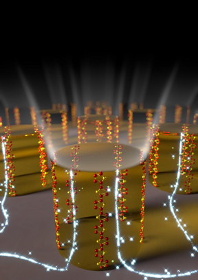 |
| Vertically aligned chains in the organic semiconducting polymer inside microscopic patterns. CREDIT: Umeĺ University |
Abstract:
A research team at Umeĺ University in Sweden has showed, for the first time, that a very efficient vertical charge transport in semiconducting polymers is possible by controlled chain and crystallite orientation. These pioneering results, which enhance charge transport in polymers by more than 1,000 times, have implications for organic opto-electronic devices and were recently published in the journal Advanced Materials.
Breakthrough enables ultra-fast transport of electrical charges in polymers
Umeĺ, Sweden | Posted on January 30th, 2016Conjugated semiconducting polymers (plastic) possess exceptional optical and electronic properties, which make them highly attractive in the production of organic opto-electronic devices, such as for instance photovoltaic solar cells (OPV), light emitting diodes (OLED) and lasers.
Polythiophene polymers, such as poly(3-hexylthiophene), P3HT, have been among the most studied semiconducting polymers due to their strong optical absorbance and ease of processing into a thin film from solution. In both OPVs and OLEDs, charges must be transported in the out of plane (vertical) direction inside the polymer film.
However, until now the vertical charge carrier mobility of organic semiconductors, i.e. the ability of charges to move inside the material, has been too low to produce fast charge transport in electronic devices. Faster charge transport can occur along the polymer chain backbone. However, a method to produce controlled chain orientation and high mobility in the vertical direction has remained elusive until now.
In the present work, a team of chemists and materials scientists, led by Professor David R. Barbero at Umeĺ University, has found a new method to align chains vertically and to produce efficient transport of electric charges through the chain backbone. In this new study, moreover, high charge transport and high mobility were obtained without any chemical doping, which is often used to artificially enhance charge transport in polymers.
"The transport of electric charge is greatly enhanced solely by controlled chain and crystallite orientation inside the film. The mobility measured was approximately one thousand times higher than previously reported in the same organic semiconductor," says David Barbero.
In what way will these results affect the field of organic electronics?
"We believe these results will impact the fields of polymer solar cells and organic photodiodes, where the charges are transported vertically in the device. Organic-based devices have traditionally been slower and less efficient than inorganic ones (e.g. made of silicon), in part due to the low mobility of organic (plastic) semiconductors. Typically, plastic semiconductors, which are only semi-crystalline, have hole mobilities about 10,000 times lower than doped silicon, which is used in many electronic devices. Now we show it is possible to obtain much higher mobility, and much closer to that of silicon, by controlled vertical chain alignment, and without doping," says David Barbero.
The charge transport was measured using nanoscopic electrical measurements, and gave a mobility averaging 3.1 cm2/V.s, which is the highest mobility ever measured in P3HT, and which comes close to a theoretical estimation of the maximum mobility in P3HT. Crystallinity and molecular packing characterisation of the polymer was performed by synchrotron X-ray diffraction at Stanford University's National Accelerator (SLAC) and confirmed that the high mobilities measured were due to the re-orientation of the polymer chains and crystallites, leading to fast charge transport along the polymer backbones.
These results, published in Advanced Materials, may open up the route to produce more efficient organic electronic devices with vertical charge transport (e.g. OPV, OLED, lasers etc.), by a simple and inexpensive method, and without requiring chemical modification of the polymer.
###
About plastics: Regular plastic materials are non-conducting, but if they contain conjugated double bonds, with delocalized electrons, which run alongside the chain backbone, they can conduct charges and transport electricity. However, these electrons (or their positive counterpart, holes) are still not as mobile as in metals or silicon, and therefore their mobility is much lower. To increase the charge mobility, the polymer is usually doped, which means introducing impurities into the material for the purpose of modulating its electrical properties.
####
For more information, please click here
Contacts:
Anna Lawrence
46-722-459-011
Copyright © Umeĺ University
If you have a comment, please Contact us.Issuers of news releases, not 7th Wave, Inc. or Nanotechnology Now, are solely responsible for the accuracy of the content.
Bookmark:


| Related Links |
| Related News Press |
News and information
![]() Quantum computer improves AI predictions April 17th, 2026
Quantum computer improves AI predictions April 17th, 2026
![]() Flexible sensor gains sensitivity under pressure April 17th, 2026
Flexible sensor gains sensitivity under pressure April 17th, 2026
![]() A reusable chip for particulate matter sensing April 17th, 2026
A reusable chip for particulate matter sensing April 17th, 2026
![]() Detecting vibrational quantum beating in the predissociation dynamics of SF6 using time-resolved photoelectron spectroscopy April 17th, 2026
Detecting vibrational quantum beating in the predissociation dynamics of SF6 using time-resolved photoelectron spectroscopy April 17th, 2026
Organic Electronics
![]() Unveiling the power of hot carriers in plasmonic nanostructures August 16th, 2024
Unveiling the power of hot carriers in plasmonic nanostructures August 16th, 2024
Laboratories
![]() Researchers develop molecular qubits that communicate at telecom frequencies October 3rd, 2025
Researchers develop molecular qubits that communicate at telecom frequencies October 3rd, 2025
Govt.-Legislation/Regulation/Funding/Policy
![]() Quantum computer improves AI predictions April 17th, 2026
Quantum computer improves AI predictions April 17th, 2026
![]() Metasurfaces smooth light to boost magnetic sensing precision January 30th, 2026
Metasurfaces smooth light to boost magnetic sensing precision January 30th, 2026
![]() New imaging approach transforms study of bacterial biofilms August 8th, 2025
New imaging approach transforms study of bacterial biofilms August 8th, 2025
Possible Futures
![]() A fundamentally new therapeutic approach to cystic fibrosis: Nanobody repairs cellular defect April 17th, 2026
A fundamentally new therapeutic approach to cystic fibrosis: Nanobody repairs cellular defect April 17th, 2026
![]() UC Irvine physicists discover method to reverse ‘quantum scrambling’ : The work addresses the problem of information loss in quantum computing system April 17th, 2026
UC Irvine physicists discover method to reverse ‘quantum scrambling’ : The work addresses the problem of information loss in quantum computing system April 17th, 2026
Chip Technology
![]() A reusable chip for particulate matter sensing April 17th, 2026
A reusable chip for particulate matter sensing April 17th, 2026
![]() Metasurfaces smooth light to boost magnetic sensing precision January 30th, 2026
Metasurfaces smooth light to boost magnetic sensing precision January 30th, 2026
Discoveries
![]() Quantum computer improves AI predictions April 17th, 2026
Quantum computer improves AI predictions April 17th, 2026
![]() Flexible sensor gains sensitivity under pressure April 17th, 2026
Flexible sensor gains sensitivity under pressure April 17th, 2026
![]() A reusable chip for particulate matter sensing April 17th, 2026
A reusable chip for particulate matter sensing April 17th, 2026
![]() Detecting vibrational quantum beating in the predissociation dynamics of SF6 using time-resolved photoelectron spectroscopy April 17th, 2026
Detecting vibrational quantum beating in the predissociation dynamics of SF6 using time-resolved photoelectron spectroscopy April 17th, 2026
Materials/Metamaterials/Magnetoresistance
![]() First real-time observation of two-dimensional melting process: Researchers at Mainz University unveil new insights into magnetic vortex structures August 8th, 2025
First real-time observation of two-dimensional melting process: Researchers at Mainz University unveil new insights into magnetic vortex structures August 8th, 2025
![]() Researchers unveil a groundbreaking clay-based solution to capture carbon dioxide and combat climate change June 6th, 2025
Researchers unveil a groundbreaking clay-based solution to capture carbon dioxide and combat climate change June 6th, 2025
![]() A 1960s idea inspires NBI researchers to study hitherto inaccessible quantum states June 6th, 2025
A 1960s idea inspires NBI researchers to study hitherto inaccessible quantum states June 6th, 2025
![]() Institute for Nanoscience hosts annual proposal planning meeting May 16th, 2025
Institute for Nanoscience hosts annual proposal planning meeting May 16th, 2025
Announcements
![]() A fundamentally new therapeutic approach to cystic fibrosis: Nanobody repairs cellular defect April 17th, 2026
A fundamentally new therapeutic approach to cystic fibrosis: Nanobody repairs cellular defect April 17th, 2026
![]() UC Irvine physicists discover method to reverse ‘quantum scrambling’ : The work addresses the problem of information loss in quantum computing system April 17th, 2026
UC Irvine physicists discover method to reverse ‘quantum scrambling’ : The work addresses the problem of information loss in quantum computing system April 17th, 2026
Interviews/Book Reviews/Essays/Reports/Podcasts/Journals/White papers/Posters
![]() A fundamentally new therapeutic approach to cystic fibrosis: Nanobody repairs cellular defect April 17th, 2026
A fundamentally new therapeutic approach to cystic fibrosis: Nanobody repairs cellular defect April 17th, 2026
![]() UC Irvine physicists discover method to reverse ‘quantum scrambling’ : The work addresses the problem of information loss in quantum computing system April 17th, 2026
UC Irvine physicists discover method to reverse ‘quantum scrambling’ : The work addresses the problem of information loss in quantum computing system April 17th, 2026
Photonics/Optics/Lasers
![]() Metasurfaces smooth light to boost magnetic sensing precision January 30th, 2026
Metasurfaces smooth light to boost magnetic sensing precision January 30th, 2026
![]() From sensors to smart systems: the rise of AI-driven photonic noses January 30th, 2026
From sensors to smart systems: the rise of AI-driven photonic noses January 30th, 2026
|
|
||
|
|
||
| The latest news from around the world, FREE | ||
|
|
||
|
|
||
| Premium Products | ||
|
|
||
|
Only the news you want to read!
Learn More |
||
|
|
||
|
Full-service, expert consulting
Learn More |
||
|
|
||