Home > Press > Nanowalls for smartphones
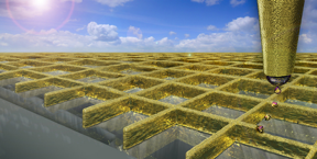 |
| With a special mode of electrohydrodynamic ink-jet printing scientists can create a grid of ultra fine gold walls. Visualisations: Ben Newton / Digit Works |
Abstract:
From smartphones to the operating interfaces of ticket machines and cash dispensers, every touchscreen we use requires transparent electrodes: The devices' glass surface is coated with a barely visible pattern made of conductive material. It is because of this that the devices recognise whether and where exactly a finger is touching the surface.
Nanowalls for smartphones
Zurich, Switzerland | Posted on January 6th, 2016Researchers under the direction of Dimos Poulikakos, Professor of Thermodynamics, have now used 3D print technology to create a new type of transparent electrode, which takes the form of a grid made of gold or silver "nanowalls" on a glass surface. The walls are so thin that they can hardly be seen with the naked eye. It is the first time that scientists have created nanowalls like these using 3D printing. The new electrodes have a higher conductivity and are more transparent than those made of indium tin oxide, the standard material used in smartphones and tablets today. This is a clear advantage: The more transparent the electrodes, the better the screen quality. And the more conductive they are, the more quickly and precisely the touchscreen will work.
Third dimension
"Indium tin oxide is used because the material has a relatively high degree of transparency and the production of thin layers has been well researched, but it is only moderately conductive," says Patrik Rohner, a PhD student in Poulikakos' team. In order to produce more conductive electrodes, the ETH researchers opted for gold and silver, which conduct electricity much better. But because these metals are not transparent, the scientists had to make use of the third dimension. ETH professor Poulikakos explains: "If you want to achieve both high conductivity and transparency in wires made from these metals, you have a conflict of objectives. As the cross-sectional area of gold and silver wires grows, the conductivity increases, but the grid's transparency decreases."
The solution was to use metal walls only 80 to 500 nanometres thick, which are almost invisible when viewed from above. Because they are two to four times taller than they are wide, the cross-sectional area, and thus the conductivity, is sufficiently high.
Ink-jet printer with tiny print head
The researchers produced these tiny metal walls using a printing process known as Nanodrip, which Poulikakos and his colleagues developed three years ago. Its basic principle is a process called electrohydrodynamic ink-jet printing. In this process scientists use inks made from metal nanoparticles in a solvent; an electrical field draws ultra-small droplets of the metallic ink out of a glass capillary. The solvent evaporates quickly, allowing a three-dimensional structure to be built up drop by drop.
What is special about the Nanodrip process is that the droplets that come out of the glass capillary are about ten times smaller than the aperture itself. This allows for much smaller structures to be printed. "Imagine a water drop hanging from a tap that is turned off. And now imagine that another tiny droplet is hanging from this drop - we are only printing the tiny droplet," Poulikakos explains. The researchers managed to create this special form of droplet by perfectly balancing the composition of metallic ink and the electromagnetic field used.
Cost-efficient production
The next big challenge will now be to upscale the method and develop the print process further so that it can be implemented on an industrial scale. To achieve this, the scientists are working with colleagues from ETH spin-off company Scrona.
They have no doubt that once it is upscaled, the technology will bring a host of advantages compared with existing methods. In particular, it will likely be more cost-efficient, as Nanodrip printing, unlike the production of indium tin oxide electrodes, does not require a cleanroom environment. The new electrodes should also be more suitable for large touchscreens due to their higher conductivity. And finally the process is also the first to allow you to vary the height of the nanowalls directly while printing, says ETH PhD student Rohner.
Another possible future application could be in solar cells, where transparent electrodes are also required. The more transparent and conductive they are, the more electricity that can be harnessed. And lastly, the electrodes could also play a role in the further development of curved display using OLED technology.
####
For more information, please click here
Contacts:
Dimos Poulikakos
41-446-322-738
Copyright © ETH Zurich
If you have a comment, please Contact us.Issuers of news releases, not 7th Wave, Inc. or Nanotechnology Now, are solely responsible for the accuracy of the content.
Bookmark:


| Related Links |
| Related News Press |
News and information
![]() Quantum computer improves AI predictions April 17th, 2026
Quantum computer improves AI predictions April 17th, 2026
![]() Flexible sensor gains sensitivity under pressure April 17th, 2026
Flexible sensor gains sensitivity under pressure April 17th, 2026
![]() A reusable chip for particulate matter sensing April 17th, 2026
A reusable chip for particulate matter sensing April 17th, 2026
![]() Detecting vibrational quantum beating in the predissociation dynamics of SF6 using time-resolved photoelectron spectroscopy April 17th, 2026
Detecting vibrational quantum beating in the predissociation dynamics of SF6 using time-resolved photoelectron spectroscopy April 17th, 2026
Display technology/LEDs/SS Lighting/OLEDs
![]() Spinel-type sulfide semiconductors to operate the next-generation LEDs and solar cells For solar-cell absorbers and green-LED source October 3rd, 2025
Spinel-type sulfide semiconductors to operate the next-generation LEDs and solar cells For solar-cell absorbers and green-LED source October 3rd, 2025
![]() Efficient and stable hybrid perovskite-organic light-emitting diodes with external quantum efficiency exceeding 40 per cent July 5th, 2024
Efficient and stable hybrid perovskite-organic light-emitting diodes with external quantum efficiency exceeding 40 per cent July 5th, 2024
Discoveries
![]() Quantum computer improves AI predictions April 17th, 2026
Quantum computer improves AI predictions April 17th, 2026
![]() Flexible sensor gains sensitivity under pressure April 17th, 2026
Flexible sensor gains sensitivity under pressure April 17th, 2026
![]() A reusable chip for particulate matter sensing April 17th, 2026
A reusable chip for particulate matter sensing April 17th, 2026
![]() Detecting vibrational quantum beating in the predissociation dynamics of SF6 using time-resolved photoelectron spectroscopy April 17th, 2026
Detecting vibrational quantum beating in the predissociation dynamics of SF6 using time-resolved photoelectron spectroscopy April 17th, 2026
Materials/Metamaterials/Magnetoresistance
![]() First real-time observation of two-dimensional melting process: Researchers at Mainz University unveil new insights into magnetic vortex structures August 8th, 2025
First real-time observation of two-dimensional melting process: Researchers at Mainz University unveil new insights into magnetic vortex structures August 8th, 2025
![]() Researchers unveil a groundbreaking clay-based solution to capture carbon dioxide and combat climate change June 6th, 2025
Researchers unveil a groundbreaking clay-based solution to capture carbon dioxide and combat climate change June 6th, 2025
![]() A 1960s idea inspires NBI researchers to study hitherto inaccessible quantum states June 6th, 2025
A 1960s idea inspires NBI researchers to study hitherto inaccessible quantum states June 6th, 2025
![]() Institute for Nanoscience hosts annual proposal planning meeting May 16th, 2025
Institute for Nanoscience hosts annual proposal planning meeting May 16th, 2025
Announcements
![]() A fundamentally new therapeutic approach to cystic fibrosis: Nanobody repairs cellular defect April 17th, 2026
A fundamentally new therapeutic approach to cystic fibrosis: Nanobody repairs cellular defect April 17th, 2026
![]() UC Irvine physicists discover method to reverse �quantum scrambling� : The work addresses the problem of information loss in quantum computing system April 17th, 2026
UC Irvine physicists discover method to reverse �quantum scrambling� : The work addresses the problem of information loss in quantum computing system April 17th, 2026
Interviews/Book Reviews/Essays/Reports/Podcasts/Journals/White papers/Posters
![]() A fundamentally new therapeutic approach to cystic fibrosis: Nanobody repairs cellular defect April 17th, 2026
A fundamentally new therapeutic approach to cystic fibrosis: Nanobody repairs cellular defect April 17th, 2026
![]() UC Irvine physicists discover method to reverse �quantum scrambling� : The work addresses the problem of information loss in quantum computing system April 17th, 2026
UC Irvine physicists discover method to reverse �quantum scrambling� : The work addresses the problem of information loss in quantum computing system April 17th, 2026
Energy
![]() Sensors innovations for smart lithium-based batteries: advancements, opportunities, and potential challenges August 8th, 2025
Sensors innovations for smart lithium-based batteries: advancements, opportunities, and potential challenges August 8th, 2025
![]() Simple algorithm paired with standard imaging tool could predict failure in lithium metal batteries August 8th, 2025
Simple algorithm paired with standard imaging tool could predict failure in lithium metal batteries August 8th, 2025
Solar/Photovoltaic
![]() Spinel-type sulfide semiconductors to operate the next-generation LEDs and solar cells For solar-cell absorbers and green-LED source October 3rd, 2025
Spinel-type sulfide semiconductors to operate the next-generation LEDs and solar cells For solar-cell absorbers and green-LED source October 3rd, 2025
![]() KAIST researchers introduce new and improved, next-generation perovskite solar cell November 8th, 2024
KAIST researchers introduce new and improved, next-generation perovskite solar cell November 8th, 2024
![]() Groundbreaking precision in single-molecule optoelectronics August 16th, 2024
Groundbreaking precision in single-molecule optoelectronics August 16th, 2024
![]() Development of zinc oxide nanopagoda array photoelectrode: photoelectrochemical water-splitting hydrogen production January 12th, 2024
Development of zinc oxide nanopagoda array photoelectrode: photoelectrochemical water-splitting hydrogen production January 12th, 2024
|
|
||
|
|
||
| The latest news from around the world, FREE | ||
|
|
||
|
|
||
| Premium Products | ||
|
|
||
|
Only the news you want to read!
Learn More |
||
|
|
||
|
Full-service, expert consulting
Learn More |
||
|
|
||