Home > Press > Alternative method for the representation of microstructures in polycrystalline materials
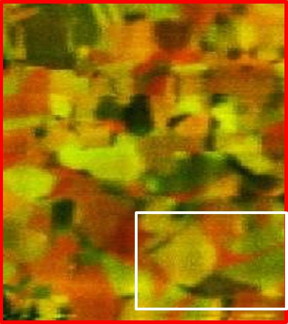 |
| This is a composite Raman intensity-distribution map on a polycrystalline CuInSe2 thin film.
CREDIT: HZB |
Abstract:
Most solid materials are of polycrystalline nature. In which way the individual grains are oriented in the material can be relevant for its functional properties. In order to determine the corresponding orientation distributions on large specimen areas, generally, a scanning electron microscope is employed. The specimen surface needs to be prepared, before it can be probed under vacuum by an electron beam and analyzed using electron backscatter diffraction (EBSD).
Alternative method for the representation of microstructures in polycrystalline materials
Berlin, Germany | Posted on December 19th, 2015It has now been shown by a team at HZB headed by Dr. Daniel Abou-Ras, together with Dr. Thomas Schmid from BAM, that equivalent orientation distribution maps can be obtained also by means of Raman microspectroscopy. This method needs only an optical microscopy setup, no time-consuming specimen preparation, and can also be conducted under ambient conditions.
The scientists used CuInSe2 thin films as a model system for their study. They showed that the experimental Raman intensities correspond well with the theoretical intensities calculated by using the local orientations from the EBSD map. "The sample area was scanned by a laser beam using step sizes of 200 nanometers. For such measurement conditions, the sample environment needs to be controlled carefully and kept stable for several hours," explains Dr. Abou-Ras.
The application of Raman microspectroscopy for orientation distribution analysis is possible in principle for all polycrystalline materials, whether they are inorganic or organic, as long as they are Raman active.
###
The report has been published in Scientific Reports: Orientation-distribution mapping of polycrystalline materials by Raman microspectroscopy, Norbert Sch�fer, Sergiu Levcenco, Daniel Abou-Ras,Thomas Schmid, Doi: 10.1038/srep18410
####
For more information, please click here
Contacts:
Dr. Daniel Abou-Ras
49-308-062-43218
Copyright © Helmholtz-Zentrum Berlin f�r Materialien und Energie
If you have a comment, please Contact us.Issuers of news releases, not 7th Wave, Inc. or Nanotechnology Now, are solely responsible for the accuracy of the content.
Bookmark:


| Related News Press |
News and information
![]() Quantum computer improves AI predictions April 17th, 2026
Quantum computer improves AI predictions April 17th, 2026
![]() Flexible sensor gains sensitivity under pressure April 17th, 2026
Flexible sensor gains sensitivity under pressure April 17th, 2026
![]() A reusable chip for particulate matter sensing April 17th, 2026
A reusable chip for particulate matter sensing April 17th, 2026
![]() Detecting vibrational quantum beating in the predissociation dynamics of SF6 using time-resolved photoelectron spectroscopy April 17th, 2026
Detecting vibrational quantum beating in the predissociation dynamics of SF6 using time-resolved photoelectron spectroscopy April 17th, 2026
Imaging
![]() Simple algorithm paired with standard imaging tool could predict failure in lithium metal batteries August 8th, 2025
Simple algorithm paired with standard imaging tool could predict failure in lithium metal batteries August 8th, 2025
![]() First real-time observation of two-dimensional melting process: Researchers at Mainz University unveil new insights into magnetic vortex structures August 8th, 2025
First real-time observation of two-dimensional melting process: Researchers at Mainz University unveil new insights into magnetic vortex structures August 8th, 2025
Thin films
![]() Tiny nanosheets, big leap: A new sensor detects ethanol at ultra-low levels January 30th, 2026
Tiny nanosheets, big leap: A new sensor detects ethanol at ultra-low levels January 30th, 2026
Discoveries
![]() Quantum computer improves AI predictions April 17th, 2026
Quantum computer improves AI predictions April 17th, 2026
![]() Flexible sensor gains sensitivity under pressure April 17th, 2026
Flexible sensor gains sensitivity under pressure April 17th, 2026
![]() A reusable chip for particulate matter sensing April 17th, 2026
A reusable chip for particulate matter sensing April 17th, 2026
![]() Detecting vibrational quantum beating in the predissociation dynamics of SF6 using time-resolved photoelectron spectroscopy April 17th, 2026
Detecting vibrational quantum beating in the predissociation dynamics of SF6 using time-resolved photoelectron spectroscopy April 17th, 2026
Announcements
![]() A fundamentally new therapeutic approach to cystic fibrosis: Nanobody repairs cellular defect April 17th, 2026
A fundamentally new therapeutic approach to cystic fibrosis: Nanobody repairs cellular defect April 17th, 2026
![]() UC Irvine physicists discover method to reverse �quantum scrambling� : The work addresses the problem of information loss in quantum computing system April 17th, 2026
UC Irvine physicists discover method to reverse �quantum scrambling� : The work addresses the problem of information loss in quantum computing system April 17th, 2026
Interviews/Book Reviews/Essays/Reports/Podcasts/Journals/White papers/Posters
![]() A fundamentally new therapeutic approach to cystic fibrosis: Nanobody repairs cellular defect April 17th, 2026
A fundamentally new therapeutic approach to cystic fibrosis: Nanobody repairs cellular defect April 17th, 2026
![]() UC Irvine physicists discover method to reverse �quantum scrambling� : The work addresses the problem of information loss in quantum computing system April 17th, 2026
UC Irvine physicists discover method to reverse �quantum scrambling� : The work addresses the problem of information loss in quantum computing system April 17th, 2026
Tools
![]() Metasurfaces smooth light to boost magnetic sensing precision January 30th, 2026
Metasurfaces smooth light to boost magnetic sensing precision January 30th, 2026
![]() From sensors to smart systems: the rise of AI-driven photonic noses January 30th, 2026
From sensors to smart systems: the rise of AI-driven photonic noses January 30th, 2026
![]() Japan launches fully domestically produced quantum computer: Expo visitors to experience quantum computing firsthand August 8th, 2025
Japan launches fully domestically produced quantum computer: Expo visitors to experience quantum computing firsthand August 8th, 2025
|
|
||
|
|
||
| The latest news from around the world, FREE | ||
|
|
||
|
|
||
| Premium Products | ||
|
|
||
|
Only the news you want to read!
Learn More |
||
|
|
||
|
Full-service, expert consulting
Learn More |
||
|
|
||