Home > Press > JPK releases the world’s most flexible AFM - the NanoWizard® 4 NanoScience AFM
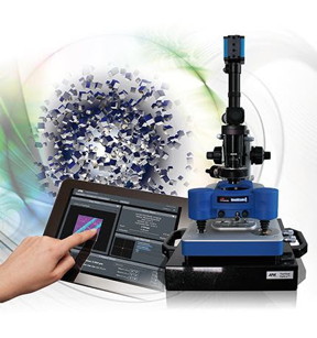 |
| JPK’s new NanoWizard® 4 NanoScience AFM |
Abstract:
JPK Instruments, a world-leading manufacturer of nanoanalytic instrumentation for research in life sciences and soft matter, announces the latest in their series of world-leading AFM systems, the NanoWizard’s 4 NanoScience AFM.
JPK releases the world’s most flexible AFM - the NanoWizard® 4 NanoScience AFM
Berlin, Germany | Posted on December 18th, 2015JPK is pleased to announce their latest AFM system, the world’s most flexible AFM: the NanoWizard® 4 NanoScience AFM. JPK continues to provide nano solutions for science. The new NanoScience system again raises the bar in terms of technical performance to deliver exciting new capabilities for users. It features a powerful fast scanning option delivering images every three seconds enabling users to track dynamic processes. Additionally, with the unique QI™ mode, quantitative imaging is possible with outstanding high resolution.
JPK have focused on providing users with easy, intuitive imaging capability with more modes and accessories than any other AFM system. Specifically, the NanoWizard® 4 NanoScience AFM provides unique solutions for mechanical and electrical sample characterization delivering flexible, advanced research capabilities to address the increasingly complex challenges faced by materials scientists today. The system employs the powerful digital Vortis™ controller to enable atomic resolution and fast scanning capabilities on a single platform. JPK's QI™ mode (based on real force curves) gives the user unmatched force sensitivity and control to be able to handle any brittle, delicate, soft or sticky sample. The proven Ultra Speed scanner technology delivers three seconds per image performance for a 100 x 100 micron image area, performance that is thirty times faster than other AFMs with such a large scan range.
With the demand for increasing productivity and with more users wishing to perform long-running experiments over prolonged periods yet still being “in contact” with them, JPK has added expanded usability and remote experimental control. The new ExperimentControl™ feature enables the user to both set up and control experiments via the Internet using their PC, tablet or smart phone. This delivers real time data allowing users to be in touch with their AFM 24/7!
The newly developed CryoStage option enables the user to control sample temperature from -120°C up to 200°C differentiating performance from regular ambient AFM systems. Additionally, the new StretchingStage can apply an external mechanical load to the sample, while the AFM measures variation of the sample properties in-situ. Furthermore, modules and modes for electrical measurements such as Conductive AFM (CAFM), Electrical Force Microscopy (EFM) and Kelvin Probe AFM (KPM-AFM) have been enhanced.
With the nano sciences constantly demanding higher performance, the NanoWizard® platform from JPK delivers a unique AFM system that has grown to meet these demands. NanoWizard® 4 NanoScience AFM is the latest solution and is designed to answer the advanced and complex questions of tomorrow's research delivered TODAY.
There is a new brochure available for downloading now. So, for more details about JPK’s NanoWizard® 4 NanoScience AFM system and its applications for the nano sciences, please contact JPK on +49 30726243 500. Alternatively, please visit the web site: www.jpk.com/ or see more on Facebook: www.jpk.com/facebook and on You Tube: www.youtube.com/jpkinstruments.
####
About JPK Instruments
JPK Instruments AG is a world-leading manufacturer of nanoanalytic instruments - particularly atomic force microscope (AFM) systems and optical tweezers - for a broad range of applications reaching from soft matter physics to nano-optics, from surface chemistry to cell and molecular biology. From its earliest days applying atomic force microscope (AFM) technology, JPK has recognized the opportunities provided by nanotechnology for transforming life sciences and soft matter research. This focus has driven JPK’s success in uniting the worlds of nanotechnology tools and life science applications by offering cutting-edge technology and unique applications expertise. Headquartered in Berlin and with direct operations in Dresden, Cambridge (UK), Singapore, Tokyo, Shanghai (China), Paris (France) and Carpinteria (USA), JPK maintains a global network of distributors and support centers and provides on the spot applications and service support to an ever-growing community of researchers.
For more information, please click here
Contacts:
JPK Instruments AG
Colditzstrasse 34-36
Haus 13, Eingang B
Berlin 12099
Germany
T +49 30726243 500
F +49 30726243 999
http://www.jpk.com/
Talking Science Limited
39 de Bohun Court
Saffron Walden
Essex CB10 2BA
United Kingdom
T +44(0)1799 521881
M +44(0)7843 012997
http://www.talking-science.com/
Copyright © JPK Instruments
If you have a comment, please Contact us.Issuers of news releases, not 7th Wave, Inc. or Nanotechnology Now, are solely responsible for the accuracy of the content.
Bookmark:


| Related News Press |
News and information
![]() Quantum computer improves AI predictions April 17th, 2026
Quantum computer improves AI predictions April 17th, 2026
![]() Flexible sensor gains sensitivity under pressure April 17th, 2026
Flexible sensor gains sensitivity under pressure April 17th, 2026
![]() A reusable chip for particulate matter sensing April 17th, 2026
A reusable chip for particulate matter sensing April 17th, 2026
![]() Detecting vibrational quantum beating in the predissociation dynamics of SF6 using time-resolved photoelectron spectroscopy April 17th, 2026
Detecting vibrational quantum beating in the predissociation dynamics of SF6 using time-resolved photoelectron spectroscopy April 17th, 2026
Imaging
![]() Simple algorithm paired with standard imaging tool could predict failure in lithium metal batteries August 8th, 2025
Simple algorithm paired with standard imaging tool could predict failure in lithium metal batteries August 8th, 2025
Announcements
![]() A fundamentally new therapeutic approach to cystic fibrosis: Nanobody repairs cellular defect April 17th, 2026
A fundamentally new therapeutic approach to cystic fibrosis: Nanobody repairs cellular defect April 17th, 2026
![]() UC Irvine physicists discover method to reverse ‘quantum scrambling’ : The work addresses the problem of information loss in quantum computing system April 17th, 2026
UC Irvine physicists discover method to reverse ‘quantum scrambling’ : The work addresses the problem of information loss in quantum computing system April 17th, 2026
Tools
![]() Metasurfaces smooth light to boost magnetic sensing precision January 30th, 2026
Metasurfaces smooth light to boost magnetic sensing precision January 30th, 2026
![]() From sensors to smart systems: the rise of AI-driven photonic noses January 30th, 2026
From sensors to smart systems: the rise of AI-driven photonic noses January 30th, 2026
![]() Japan launches fully domestically produced quantum computer: Expo visitors to experience quantum computing firsthand August 8th, 2025
Japan launches fully domestically produced quantum computer: Expo visitors to experience quantum computing firsthand August 8th, 2025
|
|
||
|
|
||
| The latest news from around the world, FREE | ||
|
|
||
|
|
||
| Premium Products | ||
|
|
||
|
Only the news you want to read!
Learn More |
||
|
|
||
|
Full-service, expert consulting
Learn More |
||
|
|
||