Home > Press > Measuring nanoscale features with fractions of light: Shows promise for next-gen semiconductor production
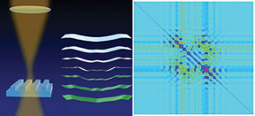 |
| Drawing illustrates how tiny changes in wavy images scattered from lines in a grid-like array can be reconstructed when paired with advanced optical and computational techniques. Lines are 15 nanometers wide, 30 times smaller than the wavelength used to �see� them. The pattern depicts estimated uncertainties in the experimental data. Coloring corresponds to the magnitude of the variance for specific data points. credit: NIST/Barnes |
Abstract:
National Institute of Standards and Technology (NIST) researchers are seeing the light, but in an altogether different way. And how they are doing it just might be the semiconductor industry's ticket for extending its use of optical microscopes to measure computer chip features that are approaching 10 nanometers, tiny fractions of the wavelength of light.
Measuring nanoscale features with fractions of light: Shows promise for next-gen semiconductor production
Gaithersburg, MD | Posted on December 3rd, 2015Using a novel microscope that combines standard through-the-lens viewing with a technique called scatterfield imaging, the NIST team accurately measured patterned features on a silicon wafer that were 30 times smaller than the wavelength of light (450 nanometers) used to examine them. They report* that measurements of the etched lines--as thin as 16 nanometers wide--on the SEMATECH-fabricated wafer were accurate to one nanometer. With the technique, they spotted variations in feature dimensions amounting to differences of a few atoms.
Measurements were confirmed by those made with an atomic force microscope, which achieves sub-nanometer resolution, but is considered too slow for online quality-control measurements. Combined with earlier results, the NIST researchers write, the new proof-of-concept study* suggests that the innovative optical approach could be a "realistic solution to a very challenging problem" facing chip makers and others aiming to harness advances in nanotechnology. All need the means for "nondestructive measurement of nanometer-scale structures with sub-nanometer sensitivity while still having high throughput.
"Light-based, or optical, microscopes can't "see" features smaller than the wavelength of light, at least not in the crisp detail necessary for making accurate measurements. However, light does scatter when it strikes so-called subwavelength features and patterned arrangements of such features. "Historically, we would ignore this scattered light because it did not yield sufficient resolution," explains Richard Silver, the physicist who initiated NIST's scatterfield imaging effort. "Now we know it contains helpful information that provides signatures telling us something about where the light came from."
With scatterfield imaging, Silver and colleagues methodically illuminate a sample with polarized light from different angles. From this collection of scattered light--nothing more than a sea of wiggly lines to the untrained eye--the NIST team can extract characteristics of the bounced lightwaves that, together, reveal the geometry of features on the specimen.
Light-scattering data are gathered in slices, which together image the volume of scattered light above and into the sample. These slices are analyzed and reconstructed to create a three-dimensional representation. The process is akin to a CT scan, except that the slices are collections of interfering waves, not cross-sectional pictures.
"It's the ensemble of data that tells us what we're after," says project leader Bryan Barnes." We may not be able see the lines on the wafer, but we can tell you what you need to know about them--their size, their shape, their spacing."
Scatterfield imaging has critical prerequisites that must be met before it can yield useful data for high-accuracy measurements of exceedingly small features. Key steps entail detailed evaluation of the path light takes as it beams through lenses, apertures and other system elements before reaching the sample. The path traversed by light scattering from the specimen undergoes the same level of scrutiny. Fortunately, scatterfield imaging lends itself to thorough characterization of both sequences of optical devices, according to the researchers. These preliminary steps are akin to error mapping so that recognized sources of inaccuracy are factored out of the data.
The method also benefits from a little advance intelligence--the as-designed arrangement of circuit lines on a chip, down to the size of individual features. Knowing what is expected to be the result of the complex chip-making process sets up a classic matchup of theory vs. experiment.
The NIST researchers can use standard equations to simulate light scattering from an ideal, defect-free pattern and, in fact, any variation thereof. Using wave analysis software they developed, the team has assembled an indexed library of light-scattering reference models. So once a specimen is scanned, the team relies on computers to compare their real-world data to models and to find close matches.
From there, succeeding rounds of analysis homes in on the remaining differences, reducing them until the only ones that remain are due to variations in geometry such as irregularities in the height, width, or shape of a line.
Measurement results achieved with the NIST approach might be said to cast light itself in an entirely new light. Their new study, the researchers say, shows that once disregarded scattered light "contains a wealth of accessible optical information."
Next steps include extending the technique to even shorter wavelengths of light, down to ultraviolet, or 193 nanometers. The aim is to accurately measure features as small as 5 nanometers.
This work is part of a larger NIST effort to supply measurement tools that enable the semiconductor industry to continue doubling the number of devices on a chip about every two years and to help other industries make products with nanoscale features. Recently, NIST and Intel researchers reported using an X-ray technique to accurately measure features on a silicon chip to within fractions of a nanometer.
####
For more information, please click here
Contacts:
Mark Bello
301-975-3776
Copyright © National Institute of Standards and Technology (NIST)
If you have a comment, please Contact us.Issuers of news releases, not 7th Wave, Inc. or Nanotechnology Now, are solely responsible for the accuracy of the content.
Bookmark:


| Related Links |
| Related News Press |
News and information
![]() Quantum computer improves AI predictions April 17th, 2026
Quantum computer improves AI predictions April 17th, 2026
![]() Flexible sensor gains sensitivity under pressure April 17th, 2026
Flexible sensor gains sensitivity under pressure April 17th, 2026
![]() A reusable chip for particulate matter sensing April 17th, 2026
A reusable chip for particulate matter sensing April 17th, 2026
![]() Detecting vibrational quantum beating in the predissociation dynamics of SF6 using time-resolved photoelectron spectroscopy April 17th, 2026
Detecting vibrational quantum beating in the predissociation dynamics of SF6 using time-resolved photoelectron spectroscopy April 17th, 2026
Imaging
![]() Simple algorithm paired with standard imaging tool could predict failure in lithium metal batteries August 8th, 2025
Simple algorithm paired with standard imaging tool could predict failure in lithium metal batteries August 8th, 2025
![]() First real-time observation of two-dimensional melting process: Researchers at Mainz University unveil new insights into magnetic vortex structures August 8th, 2025
First real-time observation of two-dimensional melting process: Researchers at Mainz University unveil new insights into magnetic vortex structures August 8th, 2025
![]() New imaging approach transforms study of bacterial biofilms August 8th, 2025
New imaging approach transforms study of bacterial biofilms August 8th, 2025
Laboratories
![]() Researchers develop molecular qubits that communicate at telecom frequencies October 3rd, 2025
Researchers develop molecular qubits that communicate at telecom frequencies October 3rd, 2025
Govt.-Legislation/Regulation/Funding/Policy
![]() Quantum computer improves AI predictions April 17th, 2026
Quantum computer improves AI predictions April 17th, 2026
![]() Metasurfaces smooth light to boost magnetic sensing precision January 30th, 2026
Metasurfaces smooth light to boost magnetic sensing precision January 30th, 2026
![]() New imaging approach transforms study of bacterial biofilms August 8th, 2025
New imaging approach transforms study of bacterial biofilms August 8th, 2025
Chip Technology
![]() A reusable chip for particulate matter sensing April 17th, 2026
A reusable chip for particulate matter sensing April 17th, 2026
![]() Metasurfaces smooth light to boost magnetic sensing precision January 30th, 2026
Metasurfaces smooth light to boost magnetic sensing precision January 30th, 2026
Discoveries
![]() Quantum computer improves AI predictions April 17th, 2026
Quantum computer improves AI predictions April 17th, 2026
![]() Flexible sensor gains sensitivity under pressure April 17th, 2026
Flexible sensor gains sensitivity under pressure April 17th, 2026
![]() A reusable chip for particulate matter sensing April 17th, 2026
A reusable chip for particulate matter sensing April 17th, 2026
![]() Detecting vibrational quantum beating in the predissociation dynamics of SF6 using time-resolved photoelectron spectroscopy April 17th, 2026
Detecting vibrational quantum beating in the predissociation dynamics of SF6 using time-resolved photoelectron spectroscopy April 17th, 2026
Announcements
![]() A fundamentally new therapeutic approach to cystic fibrosis: Nanobody repairs cellular defect April 17th, 2026
A fundamentally new therapeutic approach to cystic fibrosis: Nanobody repairs cellular defect April 17th, 2026
![]() UC Irvine physicists discover method to reverse �quantum scrambling� : The work addresses the problem of information loss in quantum computing system April 17th, 2026
UC Irvine physicists discover method to reverse �quantum scrambling� : The work addresses the problem of information loss in quantum computing system April 17th, 2026
Interviews/Book Reviews/Essays/Reports/Podcasts/Journals/White papers/Posters
![]() A fundamentally new therapeutic approach to cystic fibrosis: Nanobody repairs cellular defect April 17th, 2026
A fundamentally new therapeutic approach to cystic fibrosis: Nanobody repairs cellular defect April 17th, 2026
![]() UC Irvine physicists discover method to reverse �quantum scrambling� : The work addresses the problem of information loss in quantum computing system April 17th, 2026
UC Irvine physicists discover method to reverse �quantum scrambling� : The work addresses the problem of information loss in quantum computing system April 17th, 2026
Tools
![]() Metasurfaces smooth light to boost magnetic sensing precision January 30th, 2026
Metasurfaces smooth light to boost magnetic sensing precision January 30th, 2026
![]() From sensors to smart systems: the rise of AI-driven photonic noses January 30th, 2026
From sensors to smart systems: the rise of AI-driven photonic noses January 30th, 2026
![]() Japan launches fully domestically produced quantum computer: Expo visitors to experience quantum computing firsthand August 8th, 2025
Japan launches fully domestically produced quantum computer: Expo visitors to experience quantum computing firsthand August 8th, 2025
|
|
||
|
|
||
| The latest news from around the world, FREE | ||
|
|
||
|
|
||
| Premium Products | ||
|
|
||
|
Only the news you want to read!
Learn More |
||
|
|
||
|
Full-service, expert consulting
Learn More |
||
|
|
||