Home > Press > Stacking instead of mixing: J³lich-Aachen research team improves the energy efficiency of topological insulators
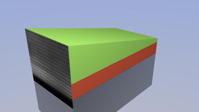 |
| By varying the thickness of the layers of semiconductor sandwiches made from silicon (grey area), bismuth-telluride, an n-type semiconductor (red area) and antimony telluride, a p-type semiconductor (green), topological insulators can be customized according to needs, as shown by the experiments conducted by researchers from J³lich and Aachen. The quality of the layers they produced using molecular beam epitaxy were verified by ultra high-resolution scanning electron microscopy. The atomic layers are clearly visible on the left side of the cube's edge. CREDIT:Forschungszentrum J³lich |
Abstract:
The overheating of computer chips is a major obstacle to the development of faster and more efficient computers and mobile phones. One promising remedy for this problem could be a class of materials first discovered just a few years ago: topological insulators, which conduct electricity with less resistance and heat generation than conventional materials. Research on these materials is still in its early stages. A team from J³lich and Aachen has now found a way to control the desired conducting properties of this type of material more precisely and reliably than ever before. The results have been published in the current edition of the journal Nature Communications (DOI: 10.1038/ncomms9816).
Stacking instead of mixing: J³lich-Aachen research team improves the energy efficiency of topological insulators
J³lich, Germany | Posted on November 21st, 2015So-called "topological" materials have different physical properties on their surface than they do on their inside. Topological insulators are in effect insulators on the inside, but on their surfaces and edges they conduct electric currents almost as if they were running along railway tracks: faster, with less resistance and less heat production than with conventional materials. Additionally, the tracks act as a one-way street for electrons. The inherent angular momentum of the electrons - known as "spin" - determines in which direction the electrons can flow. This property is also useful for information processing and can pave the way for the development of new spintronic components.
Researchers from the Peter Gr³nberg Institute and RWTH Aachen University have now shown how the conductivity and the energy requirements of these materials can be optimized. Put in highly simplified terms, their recipe for success is: stacking instead of mixing. Prof. Detlev Gr³tzmacher of the Peter Gr³nberg Institute first came up with the crucially important idea: "Instead of alloying two different types of semi-conductors as usual, in order to obtain a topological insulator, we stacked both semiconductors on top of each other, atomic layer by atomic layer, placing this in turn on a silicon backing layer with the help of molecular beam epitaxy." Molecular beam epitaxy is an extremely precise method of producing thin crystalline layers, and is increasingly used not only in research but also in the industrial production of semiconductors.
In this way, the scientists were able to control the atomic construction with great precision, which they documented with the use of ultra high-resolution electron microscopy. "Achieving the perfect atomic composition of the topological insulators is vital for the electronic properties, and thus for energy efficiency, but the alloying process is difficult to monitor", explained Dr. Lukasz Plucinski from the Peter Gr³nberg Institute.
The researchers were able to discover exactly which layer thickness goes hand in hand with optimal conduction properties using the technology of angle-resolved photoemission spectroscopy. Here, samples are bombarded with photons to trigger the release of electrons from the material. Their energy and exit angle is measured, providing information about the energy and distribution of the electrons at the sample's surface.
In principle, topological insulators can also be controlled with the help of external electric fields in semiconductor alloys and other materials. Using the sandwich method that the scientists have developed together within the framework of the J³lich Aachen Research Alliance "Future Information Technology" (JARA FIT), such complex technological procedures are no longer necessary and in addition, the silicon substrate material makes it simpler to integrate in applications at later stages.
Scientists at the Virtual Institute for Topological Insulators (VITI), coordinated by the Peter Gr³nberg Institute in J³lich, are continuing to conduct basic research on further possible uses for the new materials. This could, for example, make it possible to prove the existence of novel, only theoretically predicted quantum phenomena, such as so called topological exciton condensates, formed by electron-hole pairs at the surfaces.
####
For more information, please click here
Contacts:
Angela Wenzik
49-246-161-6048
Copyright © Forschungszentrum J³lich
If you have a comment, please Contact us.Issuers of news releases, not 7th Wave, Inc. or Nanotechnology Now, are solely responsible for the accuracy of the content.
Bookmark:


| Related News Press |
News and information
![]() Quantum computer improves AI predictions April 17th, 2026
Quantum computer improves AI predictions April 17th, 2026
![]() Flexible sensor gains sensitivity under pressure April 17th, 2026
Flexible sensor gains sensitivity under pressure April 17th, 2026
![]() A reusable chip for particulate matter sensing April 17th, 2026
A reusable chip for particulate matter sensing April 17th, 2026
![]() Detecting vibrational quantum beating in the predissociation dynamics of SF6 using time-resolved photoelectron spectroscopy April 17th, 2026
Detecting vibrational quantum beating in the predissociation dynamics of SF6 using time-resolved photoelectron spectroscopy April 17th, 2026
Chip Technology
![]() A reusable chip for particulate matter sensing April 17th, 2026
A reusable chip for particulate matter sensing April 17th, 2026
![]() Metasurfaces smooth light to boost magnetic sensing precision January 30th, 2026
Metasurfaces smooth light to boost magnetic sensing precision January 30th, 2026
Discoveries
![]() Quantum computer improves AI predictions April 17th, 2026
Quantum computer improves AI predictions April 17th, 2026
![]() Flexible sensor gains sensitivity under pressure April 17th, 2026
Flexible sensor gains sensitivity under pressure April 17th, 2026
![]() A reusable chip for particulate matter sensing April 17th, 2026
A reusable chip for particulate matter sensing April 17th, 2026
![]() Detecting vibrational quantum beating in the predissociation dynamics of SF6 using time-resolved photoelectron spectroscopy April 17th, 2026
Detecting vibrational quantum beating in the predissociation dynamics of SF6 using time-resolved photoelectron spectroscopy April 17th, 2026
Announcements
![]() A fundamentally new therapeutic approach to cystic fibrosis: Nanobody repairs cellular defect April 17th, 2026
A fundamentally new therapeutic approach to cystic fibrosis: Nanobody repairs cellular defect April 17th, 2026
![]() UC Irvine physicists discover method to reverse æquantum scramblingÆ : The work addresses the problem of information loss in quantum computing system April 17th, 2026
UC Irvine physicists discover method to reverse æquantum scramblingÆ : The work addresses the problem of information loss in quantum computing system April 17th, 2026
Interviews/Book Reviews/Essays/Reports/Podcasts/Journals/White papers/Posters
![]() A fundamentally new therapeutic approach to cystic fibrosis: Nanobody repairs cellular defect April 17th, 2026
A fundamentally new therapeutic approach to cystic fibrosis: Nanobody repairs cellular defect April 17th, 2026
![]() UC Irvine physicists discover method to reverse æquantum scramblingÆ : The work addresses the problem of information loss in quantum computing system April 17th, 2026
UC Irvine physicists discover method to reverse æquantum scramblingÆ : The work addresses the problem of information loss in quantum computing system April 17th, 2026
Quantum nanoscience
![]() Beyond silicon: Electronics at the scale of a single molecule January 30th, 2026
Beyond silicon: Electronics at the scale of a single molecule January 30th, 2026
![]() MXene nanomaterials enter a new dimension Multilayer nanomaterial: MXene flakes created at Drexel University show new promise as 1D scrolls January 30th, 2026
MXene nanomaterials enter a new dimension Multilayer nanomaterial: MXene flakes created at Drexel University show new promise as 1D scrolls January 30th, 2026
![]() ICFO researchers overcome long-standing bottleneck in single photon detection with twisted 2D materials August 8th, 2025
ICFO researchers overcome long-standing bottleneck in single photon detection with twisted 2D materials August 8th, 2025
|
|
||
|
|
||
| The latest news from around the world, FREE | ||
|
|
||
|
|
||
| Premium Products | ||
|
|
||
|
Only the news you want to read!
Learn More |
||
|
|
||
|
Full-service, expert consulting
Learn More |
||
|
|
||