Home > Press > New electron microscopy method sculpts 3-D structures at atomic level
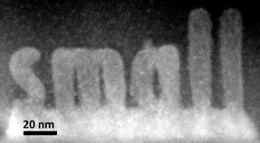 |
| ORNL researchers used a new scanning transmission electron microscopy technique to sculpt 3-D nanoscale features in a complex oxide material. CREDIT: Department of Energy's Oak Ridge National Laboratory |
Abstract:
Electron microscopy researchers at the Department of Energy's Oak Ridge National Laboratory have developed a unique way to build 3-D structures with finely controlled shapes as small as one to two billionths of a meter.
New electron microscopy method sculpts 3-D structures at atomic level
Oak Ridge, TN | Posted on November 10th, 2015The ORNL study published in the journal Small demonstrates how scanning transmission electron microscopes, normally used as imaging tools, are also capable of precision sculpting of nanometer-sized 3-D features in complex oxide materials.
By offering single atomic plane precision, the technique could find uses in fabricating structures for functional nanoscale devices such as microchips. The structures grow epitaxially, or in perfect crystalline alignment, which ensures that the same electrical and mechanical properties extend throughout the whole material.
"We can make smaller things with more precise shapes," said ORNL's Albina Borisevich, who led the study. "The process is also epitaxial, which gives us much more pronounced control over properties than we could accomplish with other approaches."
ORNL scientists happened upon the method as they were imaging an imperfectly prepared strontium titanate thin film. The sample, consisting of a crystalline substrate covered by an amorphous layer of the same material, transformed as the electron beam passed through it. A team from ORNL's Institute for Functional Imaging of Materials, which unites scientists from different disciplines, worked together to understand and exploit the discovery.
"When we exposed the amorphous layer to an electron beam, we seemed to nudge it toward adopting its preferred crystalline state," Borisevich said. "It does that exactly where the electron beam is."
The use of a scanning transmission electron microscope, which passes an electron beam through a bulk material, sets the approach apart from lithography techniques that only pattern or manipulate a material's surface.
"We're using fine control of the beam to build something inside the solid itself," said ORNL's Stephen Jesse. "We're making transformations that are buried deep within the structure. It would be like tunneling inside a mountain to build a house."
The technique offers a shortcut to researchers interested in studying how materials' characteristics change with thickness. Instead of imaging multiple samples of varying widths, scientists could use the microscopy method to add layers to the sample and simultaneously observe what happens.
"The whole premise of nanoscience is that sometimes when you shrink a material it exhibits properties that are very different than the bulk material," Borisevich said. "Here we can control that. If we know there is a certain dependence on size, we can determine exactly where we want to be on that curve and go there."
Theoretical calculations on ORNL's Titan supercomputer helped the researchers understand the process's underlying mechanisms. The simulations showed that the observed behavior, known as a knock-on process, is consistent with the electron beam transferring energy to individual atoms in the material rather than heating an area of the material.
"With the electron beam, we are injecting energy into the system and nudging where it would otherwise go by itself, given enough time," Borisevich said. "Thermodynamically it wants to be crystalline, but this process takes a long time at room temperature."
The study is published as "Atomic-level sculpting of crystalline oxides: towards bulk nanofabrication with single atomic plane precision."
###
Coauthors are ORNL's Stephen Jesse, Qian He, Andrew Lupini, Donovan Leonard, Raymond Unocic, Alexander Tselev, Miguel Fuentes-Cabrera, Bobby Sumpter, Sergei Kalinin and Albina Borisevich, Vanderbilt University's Mark Oxley and Oleg Ovchinnikov and the National University of Singapore's Stephen Pennycook.
The research was conducted as part of ORNL's Institute for Functional Imaging of Materials and was supported by DOE's Office of Science and ORNL's Laboratory Directed Research and Development program. The study used resources at ORNL's Center for Nanophase Materials Sciences and the Oak Ridge Leadership Computing Facility, which are both DOE Office of Science User Facilities.
####
About Oak Ridge National Laboratory
ORNL is managed by UT-Battelle for the Department of Energy's Office of Science. DOE's Office of Science is the single largest supporter of basic research in the physical sciences in the United States, and is working to address some of the most pressing challenges of our time. For more information, please visit science.energy.gov.
For more information, please click here
Contacts:
Morgan McCorkle
865-574-7308
Copyright © Oak Ridge National Laboratory
If you have a comment, please Contact us.Issuers of news releases, not 7th Wave, Inc. or Nanotechnology Now, are solely responsible for the accuracy of the content.
Bookmark:


| Related News Press |
News and information
![]() Quantum computer improves AI predictions April 17th, 2026
Quantum computer improves AI predictions April 17th, 2026
![]() Flexible sensor gains sensitivity under pressure April 17th, 2026
Flexible sensor gains sensitivity under pressure April 17th, 2026
![]() A reusable chip for particulate matter sensing April 17th, 2026
A reusable chip for particulate matter sensing April 17th, 2026
![]() Detecting vibrational quantum beating in the predissociation dynamics of SF6 using time-resolved photoelectron spectroscopy April 17th, 2026
Detecting vibrational quantum beating in the predissociation dynamics of SF6 using time-resolved photoelectron spectroscopy April 17th, 2026
Imaging
![]() Simple algorithm paired with standard imaging tool could predict failure in lithium metal batteries August 8th, 2025
Simple algorithm paired with standard imaging tool could predict failure in lithium metal batteries August 8th, 2025
![]() First real-time observation of two-dimensional melting process: Researchers at Mainz University unveil new insights into magnetic vortex structures August 8th, 2025
First real-time observation of two-dimensional melting process: Researchers at Mainz University unveil new insights into magnetic vortex structures August 8th, 2025
![]() New imaging approach transforms study of bacterial biofilms August 8th, 2025
New imaging approach transforms study of bacterial biofilms August 8th, 2025
Laboratories
![]() Researchers develop molecular qubits that communicate at telecom frequencies October 3rd, 2025
Researchers develop molecular qubits that communicate at telecom frequencies October 3rd, 2025
Govt.-Legislation/Regulation/Funding/Policy
![]() Quantum computer improves AI predictions April 17th, 2026
Quantum computer improves AI predictions April 17th, 2026
![]() Metasurfaces smooth light to boost magnetic sensing precision January 30th, 2026
Metasurfaces smooth light to boost magnetic sensing precision January 30th, 2026
![]() New imaging approach transforms study of bacterial biofilms August 8th, 2025
New imaging approach transforms study of bacterial biofilms August 8th, 2025
Chip Technology
![]() A reusable chip for particulate matter sensing April 17th, 2026
A reusable chip for particulate matter sensing April 17th, 2026
![]() Metasurfaces smooth light to boost magnetic sensing precision January 30th, 2026
Metasurfaces smooth light to boost magnetic sensing precision January 30th, 2026
Discoveries
![]() Quantum computer improves AI predictions April 17th, 2026
Quantum computer improves AI predictions April 17th, 2026
![]() Flexible sensor gains sensitivity under pressure April 17th, 2026
Flexible sensor gains sensitivity under pressure April 17th, 2026
![]() A reusable chip for particulate matter sensing April 17th, 2026
A reusable chip for particulate matter sensing April 17th, 2026
![]() Detecting vibrational quantum beating in the predissociation dynamics of SF6 using time-resolved photoelectron spectroscopy April 17th, 2026
Detecting vibrational quantum beating in the predissociation dynamics of SF6 using time-resolved photoelectron spectroscopy April 17th, 2026
Announcements
![]() A fundamentally new therapeutic approach to cystic fibrosis: Nanobody repairs cellular defect April 17th, 2026
A fundamentally new therapeutic approach to cystic fibrosis: Nanobody repairs cellular defect April 17th, 2026
![]() UC Irvine physicists discover method to reverse �quantum scrambling� : The work addresses the problem of information loss in quantum computing system April 17th, 2026
UC Irvine physicists discover method to reverse �quantum scrambling� : The work addresses the problem of information loss in quantum computing system April 17th, 2026
Interviews/Book Reviews/Essays/Reports/Podcasts/Journals/White papers/Posters
![]() A fundamentally new therapeutic approach to cystic fibrosis: Nanobody repairs cellular defect April 17th, 2026
A fundamentally new therapeutic approach to cystic fibrosis: Nanobody repairs cellular defect April 17th, 2026
![]() UC Irvine physicists discover method to reverse �quantum scrambling� : The work addresses the problem of information loss in quantum computing system April 17th, 2026
UC Irvine physicists discover method to reverse �quantum scrambling� : The work addresses the problem of information loss in quantum computing system April 17th, 2026
Tools
![]() Metasurfaces smooth light to boost magnetic sensing precision January 30th, 2026
Metasurfaces smooth light to boost magnetic sensing precision January 30th, 2026
![]() From sensors to smart systems: the rise of AI-driven photonic noses January 30th, 2026
From sensors to smart systems: the rise of AI-driven photonic noses January 30th, 2026
![]() Japan launches fully domestically produced quantum computer: Expo visitors to experience quantum computing firsthand August 8th, 2025
Japan launches fully domestically produced quantum computer: Expo visitors to experience quantum computing firsthand August 8th, 2025
|
|
||
|
|
||
| The latest news from around the world, FREE | ||
|
|
||
|
|
||
| Premium Products | ||
|
|
||
|
Only the news you want to read!
Learn More |
||
|
|
||
|
Full-service, expert consulting
Learn More |
||
|
|
||