Home > Press > Discovery in growing graphene nanoribbons could enable faster, more efficient electronics
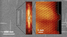 |
| Progressively zoomed-in images of graphene nanoribbons grown on germanium. The ribbons automatically align perpendicularly and naturally grow in what is known as the armchair edge configuration.
Images: Arnold Research Group and Guisinger Research Group |
Abstract:
Graphene, an atom-thick material with extraordinary properties, is a promising candidate for the next generation of dramatically faster, more energy-efficient electronics. However, scientists have struggled to fabricate the material into ultra-narrow strips, called nanoribbons, that could enable the use of graphene in high-performance semiconductor electronics.
Discovery in growing graphene nanoribbons could enable faster, more efficient electronics
Madison, WI | Posted on August 11th, 2015Now, University of Wisconsin-Madison engineers have discovered a way to grow graphene nanoribbons with desirable semiconducting properties directly on a conventional germanium semiconductor wafer. This advance could allow manufacturers to easily use graphene nanoribbons in hybrid integrated circuits, which promise to significantly boost the performance of next-generation electronic devices. The technology could also have specific uses in industrial and military applications, such as sensors that detect specific chemical and biological species and photonic devices that manipulate light.
In a paper published Aug. 10 in the journal Nature Communications, Michael Arnold, an associate professor of materials science and engineering at UW-Madison, Ph.D. student Robert Jacobberger, and their collaborators describe their new approach to producing graphene nanoribbons. Importantly, their technique can easily be scaled for mass production and is compatible with the prevailing infrastructure used in semiconductor processing.
"Graphene nanoribbons that can be grown directly on the surface of a semiconductor like germanium are more compatible with planar processing that's used in the semiconductor industry, and so there would be less of a barrier to integrating these really excellent materials into electronics in the future," Arnold says.
Graphene, a sheet of carbon atoms that is only one atom in thickness, conducts electricity and dissipates heat much more efficiently than silicon, the material most commonly found in today's computer chips. But to exploit graphene's remarkable electronic properties in semiconductor applications where current must be switched on and off, graphene nanoribbons need to be less than 10 nanometers wide, which is phenomenally narrow. In addition, the nanoribbons must have smooth, well-defined "armchair" edges in which the carbon-carbon bonds are parallel to the length of the ribbon.
Researchers have typically fabricated nanoribbons by using lithographic techniques to cut larger sheets of graphene into ribbons. However, this "top-down" fabrication approach lacks precision and produces nanoribbons with very rough edges.
Another strategy for making nanoribbons is to use a "bottom-up" approach such as surface-assisted organic synthesis, where molecular precursors react on a surface to polymerize nanoribbons. Arnold says surface-assisted synthesis can produce beautiful nanoribbons with precise, smooth edges, but this method only works on metal substrates and the resulting nanoribbons are thus far too short for use in electronics.
To overcome these hurdles, the UW-Madison researchers pioneered a bottom-up technique in which they grow ultra-narrow nanoribbons with smooth, straight edges directly on germanium wafers using a process called chemical vapor deposition. In this process, the researchers start with methane, which adsorbs to the germanium surface and decomposes to form various hydrocarbons. These hydrocarbons react with each other on the surface, where they form graphene.
Arnold's team made its discovery when it explored dramatically slowing the growth rate of the graphene crystals by decreasing the amount of methane in the chemical vapor deposition chamber. They found that at a very slow growth rate, the graphene crystals naturally grow into long nanoribbons on a specific crystal facet of germanium. By simply controlling the growth rate and growth time, the researchers can easily tune the nanoribbon width be to less than 10 nanometers.
"What we've discovered is that when graphene grows on germanium, it naturally forms nanoribbons with these very smooth, armchair edges," Arnold says. "The widths can be very, very narrow and the lengths of the ribbons can be very long, so all the desirable features we want in graphene nanoribbons are happening automatically with this technique."
The nanoribbons produced with this technique start nucleating, or growing, at seemingly random spots on the germanium and are oriented in two different directions on the surface. Arnold says the team's future work will include controlling where the ribbons start growing and aligning them all in the same direction.
The researchers are patenting their technology through the Wisconsin Alumni Research Foundation. The research was primarily supported by the Department of Energy's Basic Energy Sciences program.
###
The Arnold group worked closely with various collaborators, including Nathan Guisinger at Argonne National Laboratory, Mark C. Hersam of Northwestern University, Richard Martel of the University of Montreal, and Patrick Desjardins of Polytechnique Montreal in addition to the research groups of Paul Evans and Max Lagally in the UW-Madison Department of Materials Science and Engineering, each of whom conducted important studies to determine the structure of the nanoribbons.
�Adam Malecek,
####
For more information, please click here
Contacts:
Michael Arnold
608-262-3863
Robert Jacobberger
(402) 250-2752
Copyright © University of Wisconsin-Madison
If you have a comment, please Contact us.Issuers of news releases, not 7th Wave, Inc. or Nanotechnology Now, are solely responsible for the accuracy of the content.
Bookmark:


| Related News Press |
News and information
![]() Quantum computer improves AI predictions April 17th, 2026
Quantum computer improves AI predictions April 17th, 2026
![]() Flexible sensor gains sensitivity under pressure April 17th, 2026
Flexible sensor gains sensitivity under pressure April 17th, 2026
![]() A reusable chip for particulate matter sensing April 17th, 2026
A reusable chip for particulate matter sensing April 17th, 2026
![]() Detecting vibrational quantum beating in the predissociation dynamics of SF6 using time-resolved photoelectron spectroscopy April 17th, 2026
Detecting vibrational quantum beating in the predissociation dynamics of SF6 using time-resolved photoelectron spectroscopy April 17th, 2026
Graphene/ Graphite
![]() Electrifying results shed light on graphene foam as a potential material for lab grown cartilage June 6th, 2025
Electrifying results shed light on graphene foam as a potential material for lab grown cartilage June 6th, 2025
![]() Breakthrough in proton barrier films using pore-free graphene oxide: Kumamoto University researchers achieve new milestone in advanced coating technologies September 13th, 2024
Breakthrough in proton barrier films using pore-free graphene oxide: Kumamoto University researchers achieve new milestone in advanced coating technologies September 13th, 2024
Govt.-Legislation/Regulation/Funding/Policy
![]() Quantum computer improves AI predictions April 17th, 2026
Quantum computer improves AI predictions April 17th, 2026
![]() Metasurfaces smooth light to boost magnetic sensing precision January 30th, 2026
Metasurfaces smooth light to boost magnetic sensing precision January 30th, 2026
![]() New imaging approach transforms study of bacterial biofilms August 8th, 2025
New imaging approach transforms study of bacterial biofilms August 8th, 2025
Chip Technology
![]() A reusable chip for particulate matter sensing April 17th, 2026
A reusable chip for particulate matter sensing April 17th, 2026
![]() Metasurfaces smooth light to boost magnetic sensing precision January 30th, 2026
Metasurfaces smooth light to boost magnetic sensing precision January 30th, 2026
Discoveries
![]() Quantum computer improves AI predictions April 17th, 2026
Quantum computer improves AI predictions April 17th, 2026
![]() Flexible sensor gains sensitivity under pressure April 17th, 2026
Flexible sensor gains sensitivity under pressure April 17th, 2026
![]() A reusable chip for particulate matter sensing April 17th, 2026
A reusable chip for particulate matter sensing April 17th, 2026
![]() Detecting vibrational quantum beating in the predissociation dynamics of SF6 using time-resolved photoelectron spectroscopy April 17th, 2026
Detecting vibrational quantum beating in the predissociation dynamics of SF6 using time-resolved photoelectron spectroscopy April 17th, 2026
Materials/Metamaterials/Magnetoresistance
![]() First real-time observation of two-dimensional melting process: Researchers at Mainz University unveil new insights into magnetic vortex structures August 8th, 2025
First real-time observation of two-dimensional melting process: Researchers at Mainz University unveil new insights into magnetic vortex structures August 8th, 2025
![]() Researchers unveil a groundbreaking clay-based solution to capture carbon dioxide and combat climate change June 6th, 2025
Researchers unveil a groundbreaking clay-based solution to capture carbon dioxide and combat climate change June 6th, 2025
![]() A 1960s idea inspires NBI researchers to study hitherto inaccessible quantum states June 6th, 2025
A 1960s idea inspires NBI researchers to study hitherto inaccessible quantum states June 6th, 2025
![]() Institute for Nanoscience hosts annual proposal planning meeting May 16th, 2025
Institute for Nanoscience hosts annual proposal planning meeting May 16th, 2025
Announcements
![]() A fundamentally new therapeutic approach to cystic fibrosis: Nanobody repairs cellular defect April 17th, 2026
A fundamentally new therapeutic approach to cystic fibrosis: Nanobody repairs cellular defect April 17th, 2026
![]() UC Irvine physicists discover method to reverse �quantum scrambling� : The work addresses the problem of information loss in quantum computing system April 17th, 2026
UC Irvine physicists discover method to reverse �quantum scrambling� : The work addresses the problem of information loss in quantum computing system April 17th, 2026
Grants/Sponsored Research/Awards/Scholarships/Gifts/Contests/Honors/Records
![]() Quantum computer improves AI predictions April 17th, 2026
Quantum computer improves AI predictions April 17th, 2026
![]() Detecting vibrational quantum beating in the predissociation dynamics of SF6 using time-resolved photoelectron spectroscopy April 17th, 2026
Detecting vibrational quantum beating in the predissociation dynamics of SF6 using time-resolved photoelectron spectroscopy April 17th, 2026
![]() Metasurfaces smooth light to boost magnetic sensing precision January 30th, 2026
Metasurfaces smooth light to boost magnetic sensing precision January 30th, 2026
Research partnerships
![]() Lab to industry: InSe wafer-scale breakthrough for future electronics August 8th, 2025
Lab to industry: InSe wafer-scale breakthrough for future electronics August 8th, 2025
![]() HKU physicists uncover hidden order in the quantum world through deconfined quantum critical points April 25th, 2025
HKU physicists uncover hidden order in the quantum world through deconfined quantum critical points April 25th, 2025
|
|
||
|
|
||
| The latest news from around the world, FREE | ||
|
|
||
|
|
||
| Premium Products | ||
|
|
||
|
Only the news you want to read!
Learn More |
||
|
|
||
|
Full-service, expert consulting
Learn More |
||
|
|
||