Home > Press > Transparent, electrically conductive network of encapsulated silver nanowires: A novel electrode for optoelectronics
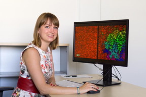 |
| Manuela G�belt is evaluating SEM-images to calculate the local degree of networking. CREDIT: Photo: Bj�rn Hoffmann. |
Abstract:
The electrodes for connections on the "sunny side" of a solar cell need to be not just electrically conductive, but transparent as well. As a result, electrodes are currently made either by using thin strips of silver in the form of a coarse-meshed grid squeegeed onto a surface, or by applying a transparent layer of electrically conductive indium tin oxide (ITO) compound. Neither of these are ideal solutions, however. This is because silver is a precious metal and relatively expensive, and silver particles with nanoscale dimensions oxidise particularly rapidly; meanwhile, indium is one of the rarest elements on earth crust and probably will only continue to be available for a few more years.
Transparent, electrically conductive network of encapsulated silver nanowires: A novel electrode for optoelectronics
Berlin, Germany | Posted on August 1st, 2015Mesh of silver nanowires
Manuela G�belt on the team of Prof. Silke Christiansen has now developed an elegant new solution using only a fraction of the silver and entirely devoid of indium to produce a technologically intriguing electrode. The doctoral student initially made a suspension of silver nanowires in ethanol using wet-chemistry techniques. She then transferred this suspension with a pipette onto a substrate, in this case a silicon solar cell. As the solvent is evaporated, the silver nanowires organise themselves into a loose mesh that remains transparent, yet dense enough to form uninterrupted current paths.
Encapsulation by AZO crystals
Subsequently, G�belt used an atomic layer deposition technique to gradually apply a coating of a highly doped wide bandgap semiconductor known as AZO. AZO consists of zinc oxide that is doped with aluminium. It is much less expensive than ITO and just as transparent, but not quite as electrically conductive. This process caused tiny AZO crystals to form on the silver nanowires, enveloped them completely, and finally filled in the interstices. The silver nanowires, measuring about 120 nanometres in diameter, were covered with a layer of about 100 nanometres of AZO and encapsulated by this process.
Quality map calculated
Measurements of the electrical conductivity showed that the newly developed composite electrode is comparable to a conventional silver grid electrode. However, its performance depends on how well the nanowires are interconnected, which is a function of the wire lengths and the concentration of silver nanowires in the suspension. The scientists were able to specify the degree of networking in advance with computers. Using specially developed image analysis algorithms, they could evaluate images taken with a scanning electron microscope and predict the electrical conductivity of the electrodes from them.
"We are investigating where a given continuous conductive path of nanowires is interrupted to see where the network is not yet optimum", explains Ralf Keding. Even with high-performance computers, it still initially took nearly five days to calculate a good "quality map" of the electrode. The software is now being optimised to reduce the computation time. "The image analysis has given us valuable clues about where we need to concentrate our efforts to increase the performance of the electrode, such as increased networking to improve areas of poor coverage by changing the wire lengths or the wire concentration in solution", says G�belt.
Practical aternative to conventional electrodes
"We have developed a practical, cost-effective alternative to conventional screen-printed grid electrodes and to the common ITO type that is threatened however by material bottlenecks", says Christiansen, who heads the Institute of Nanoarchitectures for Energy Conversion at HZB and additionally directs a project team at the Max Planck Institute for the Science of Light (MPL).
Only a fraction of silver, nearly no shadow effects
The new electrodes can actually be made using only 0.3 grams of silver per square metre, while conventional silver grid electrodes require closer to between 15 and 20 grams of silver. In addition, the new electrode casts a considerably smaller shadow on the solar cell. "The network of silver nanowires is so fine that almost no light for solar energy conversion is lost in the cell due to the shadow", explains G�belt. On the contrary, she hopes "it might even be possible for the silver nanowires to scatter light into the solar cell absorbers in a controlled fashion through what are known as plasmonic effects."
###
Published in Nano Energy, Vol. 16, Sept. 2015: "Encapsulation of silver nanowire networks by atomic layer deposition for indium-free transparent electrodes". Manuela G�belt, Ralf Keding, Sebastian W. Schmitt,Bj�rn Hoffmann, Sara J�ckle, Michael Latzel, Vuk V. Radmilovi, Velimir R. Radmilovi, Erdmann Spiecker, Silke Christiansen.
doi:10.1016/j.nanoen.2015.06.027
####
For more information, please click here
Contacts:
Manuela Goebelt
49-091-316-877-551
Copyright © Helmholtz-Zentrum Berlin f�r Materialien und Energie
If you have a comment, please Contact us.Issuers of news releases, not 7th Wave, Inc. or Nanotechnology Now, are solely responsible for the accuracy of the content.
Bookmark:


| Related News Press |
News and information
![]() Quantum computer improves AI predictions April 17th, 2026
Quantum computer improves AI predictions April 17th, 2026
![]() Flexible sensor gains sensitivity under pressure April 17th, 2026
Flexible sensor gains sensitivity under pressure April 17th, 2026
![]() A reusable chip for particulate matter sensing April 17th, 2026
A reusable chip for particulate matter sensing April 17th, 2026
![]() Detecting vibrational quantum beating in the predissociation dynamics of SF6 using time-resolved photoelectron spectroscopy April 17th, 2026
Detecting vibrational quantum beating in the predissociation dynamics of SF6 using time-resolved photoelectron spectroscopy April 17th, 2026
Discoveries
![]() Quantum computer improves AI predictions April 17th, 2026
Quantum computer improves AI predictions April 17th, 2026
![]() Flexible sensor gains sensitivity under pressure April 17th, 2026
Flexible sensor gains sensitivity under pressure April 17th, 2026
![]() A reusable chip for particulate matter sensing April 17th, 2026
A reusable chip for particulate matter sensing April 17th, 2026
![]() Detecting vibrational quantum beating in the predissociation dynamics of SF6 using time-resolved photoelectron spectroscopy April 17th, 2026
Detecting vibrational quantum beating in the predissociation dynamics of SF6 using time-resolved photoelectron spectroscopy April 17th, 2026
Materials/Metamaterials/Magnetoresistance
![]() First real-time observation of two-dimensional melting process: Researchers at Mainz University unveil new insights into magnetic vortex structures August 8th, 2025
First real-time observation of two-dimensional melting process: Researchers at Mainz University unveil new insights into magnetic vortex structures August 8th, 2025
![]() Researchers unveil a groundbreaking clay-based solution to capture carbon dioxide and combat climate change June 6th, 2025
Researchers unveil a groundbreaking clay-based solution to capture carbon dioxide and combat climate change June 6th, 2025
![]() A 1960s idea inspires NBI researchers to study hitherto inaccessible quantum states June 6th, 2025
A 1960s idea inspires NBI researchers to study hitherto inaccessible quantum states June 6th, 2025
![]() Institute for Nanoscience hosts annual proposal planning meeting May 16th, 2025
Institute for Nanoscience hosts annual proposal planning meeting May 16th, 2025
Announcements
![]() A fundamentally new therapeutic approach to cystic fibrosis: Nanobody repairs cellular defect April 17th, 2026
A fundamentally new therapeutic approach to cystic fibrosis: Nanobody repairs cellular defect April 17th, 2026
![]() UC Irvine physicists discover method to reverse �quantum scrambling� : The work addresses the problem of information loss in quantum computing system April 17th, 2026
UC Irvine physicists discover method to reverse �quantum scrambling� : The work addresses the problem of information loss in quantum computing system April 17th, 2026
Interviews/Book Reviews/Essays/Reports/Podcasts/Journals/White papers/Posters
![]() A fundamentally new therapeutic approach to cystic fibrosis: Nanobody repairs cellular defect April 17th, 2026
A fundamentally new therapeutic approach to cystic fibrosis: Nanobody repairs cellular defect April 17th, 2026
![]() UC Irvine physicists discover method to reverse �quantum scrambling� : The work addresses the problem of information loss in quantum computing system April 17th, 2026
UC Irvine physicists discover method to reverse �quantum scrambling� : The work addresses the problem of information loss in quantum computing system April 17th, 2026
Energy
![]() Sensors innovations for smart lithium-based batteries: advancements, opportunities, and potential challenges August 8th, 2025
Sensors innovations for smart lithium-based batteries: advancements, opportunities, and potential challenges August 8th, 2025
![]() Simple algorithm paired with standard imaging tool could predict failure in lithium metal batteries August 8th, 2025
Simple algorithm paired with standard imaging tool could predict failure in lithium metal batteries August 8th, 2025
Solar/Photovoltaic
![]() Spinel-type sulfide semiconductors to operate the next-generation LEDs and solar cells For solar-cell absorbers and green-LED source October 3rd, 2025
Spinel-type sulfide semiconductors to operate the next-generation LEDs and solar cells For solar-cell absorbers and green-LED source October 3rd, 2025
![]() KAIST researchers introduce new and improved, next-generation perovskite solar cell November 8th, 2024
KAIST researchers introduce new and improved, next-generation perovskite solar cell November 8th, 2024
![]() Groundbreaking precision in single-molecule optoelectronics August 16th, 2024
Groundbreaking precision in single-molecule optoelectronics August 16th, 2024
![]() Development of zinc oxide nanopagoda array photoelectrode: photoelectrochemical water-splitting hydrogen production January 12th, 2024
Development of zinc oxide nanopagoda array photoelectrode: photoelectrochemical water-splitting hydrogen production January 12th, 2024
|
|
||
|
|
||
| The latest news from around the world, FREE | ||
|
|
||
|
|
||
| Premium Products | ||
|
|
||
|
Only the news you want to read!
Learn More |
||
|
|
||
|
Full-service, expert consulting
Learn More |
||
|
|
||