Home > Press > Nanowires could be the LEDs of the future
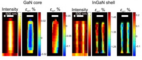 |
| The X-ray images of each nanowire show the distribution of the scattering intensity and the mechanical strain in the core of gallium-nitride and the shell of indium-gallium-nitride. The strain shows that the shell fits perfectly with the core.
Credit: Tomas Stankevic, Niels Bohr Institute, University of Copenhagen. |
Abstract:
The latest research from the Niels Bohr Institute shows that LEDs made from nanowires will use less energy and provide better light. The researchers studied nanowires using X-ray microscopy and with this method they can pinpoint exactly how the nanowire should be designed to give the best properties. The results are published in the scientific journal, ACS Nano.
Nanowires could be the LEDs of the future
Copenhagen, Denmark | Posted on June 25th, 2015Nanowires are very small - about 2 micrometers high (1 micrometer is a thousandth of a millimetre) and 10-500 nanometers in diameter (1 nanometer is a thousandth of a micrometer). Nanowires for LEDs are made up of an inner core of gallium nitride (GaN) and a layer of indium-gallium-nitride (InGaN) on the outside, both of which are semiconducting materials.
"The light in such a diode is dependent on the mechanical strain that exists between the two materials and the strain is very dependent on how the two layers are in contact with each other. We have examined a number of nanowires using X-ray microscopy and even though the nanowires should in principle be identical, we can see that they are different and have very different structure," explains Robert Feidenhans'l, professor and head of the Niels Bohr Institute at the University of Copenhagen.
Surprisingly efficient
The studies were performed using nanoscale X-ray microscopy in the electron synchrotron at DESY in Hamburg, Germany. The method is usually very time consuming and the results are often limited to very few or even a single study subject. But here researchers have managed to measure a series of upright nanowires all at once using a special design of a nanofocused X-ray without destroying the nanowires in the process.
"We measured 20 nanowires and when we saw the images, we were very surprised because you could clearly see the details of each nanowire. You can see the structure of both the inner core and the outer layer. If there are defects in the structure or if they are slightly bent, they do not function as well. So we can identify exactly which nanowires are the best and have the most efficient core/shell structure," explains Tomas Stankevic, a PhD student in the research group 'Neutron and X-ray Scattering' at the Niels Bohr Institute at the University of Copenhagen.
The nanowires are produced by a company in Sweden and this new information can be used to tweak the layer structure in the nanowires. Professor Robert Feidenhans'l explains that there is great potential in such nanowires. They will provide a more natural light in LEDs and they will use much less power. In addition, they could be used in smart phones, televisions and many forms of lighting.
The researchers expect that things could go very quickly and that they may already be in use within five years.
####
For more information, please click here
Contacts:
Gertie Skaarup
45-28-75-06-20
Robert Feidenhans'l
Professor
Head of Institute
Niels Bohr Institute
University of Copenhagen
+45 2875-0397
Tomas Stankevic, PhD-stud.
Niels Bohr Institute
University of Copenhagen
+45 9111-1486
Copyright © University of Copenhagen - Niels Bohr Institute
If you have a comment, please Contact us.Issuers of news releases, not 7th Wave, Inc. or Nanotechnology Now, are solely responsible for the accuracy of the content.
Bookmark:


| Related Links |
| Related News Press |
News and information
![]() Quantum computer improves AI predictions April 17th, 2026
Quantum computer improves AI predictions April 17th, 2026
![]() Flexible sensor gains sensitivity under pressure April 17th, 2026
Flexible sensor gains sensitivity under pressure April 17th, 2026
![]() A reusable chip for particulate matter sensing April 17th, 2026
A reusable chip for particulate matter sensing April 17th, 2026
![]() Detecting vibrational quantum beating in the predissociation dynamics of SF6 using time-resolved photoelectron spectroscopy April 17th, 2026
Detecting vibrational quantum beating in the predissociation dynamics of SF6 using time-resolved photoelectron spectroscopy April 17th, 2026
Imaging
![]() Simple algorithm paired with standard imaging tool could predict failure in lithium metal batteries August 8th, 2025
Simple algorithm paired with standard imaging tool could predict failure in lithium metal batteries August 8th, 2025
![]() First real-time observation of two-dimensional melting process: Researchers at Mainz University unveil new insights into magnetic vortex structures August 8th, 2025
First real-time observation of two-dimensional melting process: Researchers at Mainz University unveil new insights into magnetic vortex structures August 8th, 2025
![]() New imaging approach transforms study of bacterial biofilms August 8th, 2025
New imaging approach transforms study of bacterial biofilms August 8th, 2025
Display technology/LEDs/SS Lighting/OLEDs
![]() Spinel-type sulfide semiconductors to operate the next-generation LEDs and solar cells For solar-cell absorbers and green-LED source October 3rd, 2025
Spinel-type sulfide semiconductors to operate the next-generation LEDs and solar cells For solar-cell absorbers and green-LED source October 3rd, 2025
Nanoelectronics
![]() Lab to industry: InSe wafer-scale breakthrough for future electronics August 8th, 2025
Lab to industry: InSe wafer-scale breakthrough for future electronics August 8th, 2025
![]() Interdisciplinary: Rice team tackles the future of semiconductors Multiferroics could be the key to ultralow-energy computing October 6th, 2023
Interdisciplinary: Rice team tackles the future of semiconductors Multiferroics could be the key to ultralow-energy computing October 6th, 2023
![]() Key element for a scalable quantum computer: Physicists from Forschungszentrum J�lich and RWTH Aachen University demonstrate electron transport on a quantum chip September 23rd, 2022
Key element for a scalable quantum computer: Physicists from Forschungszentrum J�lich and RWTH Aachen University demonstrate electron transport on a quantum chip September 23rd, 2022
![]() Reduced power consumption in semiconductor devices September 23rd, 2022
Reduced power consumption in semiconductor devices September 23rd, 2022
Discoveries
![]() Quantum computer improves AI predictions April 17th, 2026
Quantum computer improves AI predictions April 17th, 2026
![]() Flexible sensor gains sensitivity under pressure April 17th, 2026
Flexible sensor gains sensitivity under pressure April 17th, 2026
![]() A reusable chip for particulate matter sensing April 17th, 2026
A reusable chip for particulate matter sensing April 17th, 2026
![]() Detecting vibrational quantum beating in the predissociation dynamics of SF6 using time-resolved photoelectron spectroscopy April 17th, 2026
Detecting vibrational quantum beating in the predissociation dynamics of SF6 using time-resolved photoelectron spectroscopy April 17th, 2026
Announcements
![]() A fundamentally new therapeutic approach to cystic fibrosis: Nanobody repairs cellular defect April 17th, 2026
A fundamentally new therapeutic approach to cystic fibrosis: Nanobody repairs cellular defect April 17th, 2026
![]() UC Irvine physicists discover method to reverse �quantum scrambling� : The work addresses the problem of information loss in quantum computing system April 17th, 2026
UC Irvine physicists discover method to reverse �quantum scrambling� : The work addresses the problem of information loss in quantum computing system April 17th, 2026
Interviews/Book Reviews/Essays/Reports/Podcasts/Journals/White papers/Posters
![]() A fundamentally new therapeutic approach to cystic fibrosis: Nanobody repairs cellular defect April 17th, 2026
A fundamentally new therapeutic approach to cystic fibrosis: Nanobody repairs cellular defect April 17th, 2026
![]() UC Irvine physicists discover method to reverse �quantum scrambling� : The work addresses the problem of information loss in quantum computing system April 17th, 2026
UC Irvine physicists discover method to reverse �quantum scrambling� : The work addresses the problem of information loss in quantum computing system April 17th, 2026
Tools
![]() Metasurfaces smooth light to boost magnetic sensing precision January 30th, 2026
Metasurfaces smooth light to boost magnetic sensing precision January 30th, 2026
![]() From sensors to smart systems: the rise of AI-driven photonic noses January 30th, 2026
From sensors to smart systems: the rise of AI-driven photonic noses January 30th, 2026
![]() Japan launches fully domestically produced quantum computer: Expo visitors to experience quantum computing firsthand August 8th, 2025
Japan launches fully domestically produced quantum computer: Expo visitors to experience quantum computing firsthand August 8th, 2025
|
|
||
|
|
||
| The latest news from around the world, FREE | ||
|
|
||
|
|
||
| Premium Products | ||
|
|
||
|
Only the news you want to read!
Learn More |
||
|
|
||
|
Full-service, expert consulting
Learn More |
||
|
|
||