Home > Press > Futuristic components on silicon chips, fabricated successfully
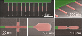 |
| Scanning electron microscope images of single crystal structures fabricated using template-assisted selective epitaxy are shown. For better visibility, the silicon is colored in green, and the compound semiconductor in red. CREDIT: H. Schmid/IBM |
Abstract:
A team of IBM researchers in Zurich, Switzerland with support from colleagues in Yorktown Heights, New York has developed a relatively simple, robust and versatile process for growing crystals made from compound semiconductor materials that will allow them be integrated onto silicon wafers -- an important step toward making future computer chips that will allow integrated circuits to continue shrinking in size and cost even as they increase in performance.
Futuristic components on silicon chips, fabricated successfully
Washington, DC | Posted on June 8th, 2015Appearing this week on the cover of the journal Applied Physics Letters, from AIP Publishing, the work may allow an extension to Moore's Law, the famous observation by Gordon Moore that the number of transistors on an integrated circuit double about every two years. In recent years some in the industry have speculated that our ability to keep pace with Moore's Law may become exhausted eventually unless new technologies come along that will lend it leash.
"The whole semiconductor industry wants to keep Moore's Law going. We need better performing transistors as we continue down-scaling, and transistors based on silicon won't give us improvements anymore," said Heinz Schmid, a researcher with IBM Research GmbH at Zurich Research Laboratory in Switzerland and the lead author on the paper.
For consumers, extending Moore's Law will mean continuing the trend of new computer devices having increasing speed and bandwidth at reduced power consumption and cost. The new technique may also impact photonics on silicon, with active photonic components integrated seamlessly with electronics for greater functionality.
How the Work was Done
The IBM team fabricated single crystal nanostructures, such as nanowires, nanostructures containing constrictions, and cross junctions, as well as 3-D stacked nanowires, made with so-called III-V materials. Made from alloys of indium, gallium and arsenide, III-V semiconductors are seen as a possible future material for computer chips, but only if they can be successfully integrated onto silicon. So far efforts at integration have not been very successful.
The new crystals were grown using an approach called template-assisted selective epitaxy (TASE) using metal organic chemical vapor deposition, which basically starts from a small area and evolves into a much larger, defect-free crystal. This approach allowed them to lithographically define oxide templates and fill them via epitaxy, in the end making nanowires, cross junctions, nanostructures containing constrictions and 3-D stacked nanowires using the already established scaled processes of Si technology.
"What sets this work apart from other methods is that the compound semiconductor does not contain detrimental defects, and that the process is fully compatible with current chip fabrication technology," said Schmid. "Importantly the method is also economically viable."
He added that more development will be required to achieve the same control over performance in III-V devices as currently exists for silicon. But the new method is the key to actually integrating the stacked materials on the silicon platform, Schmid said.
####
About American Institute of Physics
Applied Physics Letters features concise, rapid reports on significant new findings in applied physics. The journal covers new experimental and theoretical research on applications of physics phenomena related to all branches of science, engineering, and modern technology. See: apl.aip.org
For more information, please click here
Contacts:
Jason Socrates Bardi
240-535-4954
Copyright © American Institute of Physics
If you have a comment, please Contact us.Issuers of news releases, not 7th Wave, Inc. or Nanotechnology Now, are solely responsible for the accuracy of the content.
Bookmark:


| Related Links |
| Related News Press |
News and information
![]() Quantum computer improves AI predictions April 17th, 2026
Quantum computer improves AI predictions April 17th, 2026
![]() Flexible sensor gains sensitivity under pressure April 17th, 2026
Flexible sensor gains sensitivity under pressure April 17th, 2026
![]() A reusable chip for particulate matter sensing April 17th, 2026
A reusable chip for particulate matter sensing April 17th, 2026
![]() Detecting vibrational quantum beating in the predissociation dynamics of SF6 using time-resolved photoelectron spectroscopy April 17th, 2026
Detecting vibrational quantum beating in the predissociation dynamics of SF6 using time-resolved photoelectron spectroscopy April 17th, 2026
Physics
![]() UC Irvine physicists discover method to reverse �quantum scrambling� : The work addresses the problem of information loss in quantum computing system April 17th, 2026
UC Irvine physicists discover method to reverse �quantum scrambling� : The work addresses the problem of information loss in quantum computing system April 17th, 2026
![]() Quantum computers simulate fundamental physics: shedding light on the building blocks of nature June 6th, 2025
Quantum computers simulate fundamental physics: shedding light on the building blocks of nature June 6th, 2025
Chip Technology
![]() A reusable chip for particulate matter sensing April 17th, 2026
A reusable chip for particulate matter sensing April 17th, 2026
![]() Metasurfaces smooth light to boost magnetic sensing precision January 30th, 2026
Metasurfaces smooth light to boost magnetic sensing precision January 30th, 2026
Nanoelectronics
![]() Lab to industry: InSe wafer-scale breakthrough for future electronics August 8th, 2025
Lab to industry: InSe wafer-scale breakthrough for future electronics August 8th, 2025
![]() Interdisciplinary: Rice team tackles the future of semiconductors Multiferroics could be the key to ultralow-energy computing October 6th, 2023
Interdisciplinary: Rice team tackles the future of semiconductors Multiferroics could be the key to ultralow-energy computing October 6th, 2023
![]() Key element for a scalable quantum computer: Physicists from Forschungszentrum J�lich and RWTH Aachen University demonstrate electron transport on a quantum chip September 23rd, 2022
Key element for a scalable quantum computer: Physicists from Forschungszentrum J�lich and RWTH Aachen University demonstrate electron transport on a quantum chip September 23rd, 2022
![]() Reduced power consumption in semiconductor devices September 23rd, 2022
Reduced power consumption in semiconductor devices September 23rd, 2022
Discoveries
![]() Quantum computer improves AI predictions April 17th, 2026
Quantum computer improves AI predictions April 17th, 2026
![]() Flexible sensor gains sensitivity under pressure April 17th, 2026
Flexible sensor gains sensitivity under pressure April 17th, 2026
![]() A reusable chip for particulate matter sensing April 17th, 2026
A reusable chip for particulate matter sensing April 17th, 2026
![]() Detecting vibrational quantum beating in the predissociation dynamics of SF6 using time-resolved photoelectron spectroscopy April 17th, 2026
Detecting vibrational quantum beating in the predissociation dynamics of SF6 using time-resolved photoelectron spectroscopy April 17th, 2026
Announcements
![]() A fundamentally new therapeutic approach to cystic fibrosis: Nanobody repairs cellular defect April 17th, 2026
A fundamentally new therapeutic approach to cystic fibrosis: Nanobody repairs cellular defect April 17th, 2026
![]() UC Irvine physicists discover method to reverse �quantum scrambling� : The work addresses the problem of information loss in quantum computing system April 17th, 2026
UC Irvine physicists discover method to reverse �quantum scrambling� : The work addresses the problem of information loss in quantum computing system April 17th, 2026
Interviews/Book Reviews/Essays/Reports/Podcasts/Journals/White papers/Posters
![]() A fundamentally new therapeutic approach to cystic fibrosis: Nanobody repairs cellular defect April 17th, 2026
A fundamentally new therapeutic approach to cystic fibrosis: Nanobody repairs cellular defect April 17th, 2026
![]() UC Irvine physicists discover method to reverse �quantum scrambling� : The work addresses the problem of information loss in quantum computing system April 17th, 2026
UC Irvine physicists discover method to reverse �quantum scrambling� : The work addresses the problem of information loss in quantum computing system April 17th, 2026
Research partnerships
![]() Lab to industry: InSe wafer-scale breakthrough for future electronics August 8th, 2025
Lab to industry: InSe wafer-scale breakthrough for future electronics August 8th, 2025
![]() HKU physicists uncover hidden order in the quantum world through deconfined quantum critical points April 25th, 2025
HKU physicists uncover hidden order in the quantum world through deconfined quantum critical points April 25th, 2025
|
|
||
|
|
||
| The latest news from around the world, FREE | ||
|
|
||
|
|
||
| Premium Products | ||
|
|
||
|
Only the news you want to read!
Learn More |
||
|
|
||
|
Full-service, expert consulting
Learn More |
||
|
|
||