Home > Press > Two-dimensional semiconductor comes clean
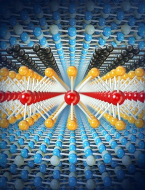 |
| This is a schematic cross-section view of atomic layer of molybdenum disulfide contacted by graphene, and encapsulated between layers of insulating hexagonal boron nitride. CREDIT: Gwan-Hyoung Lee/Columbia Engineering |
Abstract:
In 2013 James Hone, Wang Fong-Jen Professor of Mechanical Engineering at Columbia Engineering, and colleagues at Columbia demonstrated that they could dramatically improve the performance of graphene--highly conducting two-dimensional (2D) carbon--by encapsulating it in boron nitride (BN), an insulating material with a similar layered structure. In work published this week in the Advance Online Publication on Nature Nanotechnology's website, researchers at Columbia Engineering, Harvard, Cornell, University of Minnesota, Yonsei University in Korea, Danish Technical University, and the Japanese National Institute of Materials Science have shown that the performance of another 2D material--molybdenum disulfide (MoS2)--can be similarly improved by BN-encapsulation.
Two-dimensional semiconductor comes clean
New York, NY | Posted on April 27th, 2015"These findings provide a demonstration of how to study all 2D materials," says Hone, leader of this new study and director of Columbia's NSF-funded Materials Research Science and Engineering Center. "Our combination of BN and graphene electrodes is like a 'socket' into which we can place many other materials and study them in an extremely clean environment to understand their true properties and potential. This holds great promise for a broad range of applications including high-performance electronics, detection and emission of light, and chemical/bio-sensing."
Two-dimensional (2D) materials created by "peeling'" atomically thin layers from bulk crystals are extremely stretchable, optically transparent, and can be combined with each other and with conventional electronics in entirely new ways. But these materials--in which all atoms are at the surface--are by their nature extremely sensitive to their environment, and their performance often falls far short of theoretical limits due to contamination and trapped charges in surrounding insulating layers. The BN-encapsulated graphene that Hone's group produced last year has 50� improved electronic mobility--an important measure of electronic performance--and lower disorder that enables the study of rich new phenomena at low temperature and high magnetic fields.
"We wanted to see what we could do with MoS2--it's the best-studied 2D semiconductor, and, unlike graphene, it can form a transistor that can be switched fully 'off', a property crucial for digital circuits," notes Gwan-Hyoung Lee, co-lead author on the paper and assistant professor of materials science at Yonsei. In the past, MoS2 devices made on common insulating substrates such as silicon dioxide have shown mobility that falls below theoretical predictions, varies from sample to sample, and remains low upon cooling to low temperatures, all indications of a disordered material. Researchers have not known whether the disorder was due to the substrate, as in the case of graphene, or due to imperfections in the material itself.
In the new work, Hone's team created heterostructures, or layered stacks, of MoS2 encapsulated in BN, with small flakes of graphene overlapping the edge of the MoS2 to act as electrical contacts. They found that the room-temperature mobility was improved by a factor of about 2, approaching the intrinsic limit. Upon cooling to low temperature, the mobility increased dramatically, reaching values 5-50� that those measured previously (depending on the number of atomic layers). As a further sign of low disorder, these high-mobility samples also showed strong oscillations in resistance with magnetic field, which had not been previously seen in any 2D semiconductor.
"This new device structure enables us to study quantum transport behavior in this material at low temperature for the first time," added Columbia Engineering PhD student Xu Cui, the first author of the paper.
By analyzing the low-temperature resistance and quantum oscillations, the team was able to conclude that the main source of disorder remains contamination at the interfaces, indicating that further improvements are possible.
"This work motivates us to further improve our device assembly techniques, since we have not yet reached the intrinsic limit for this material," Hone says. "With further progress, we hope to establish 2D semiconductors as a new family of electronic materials that rival the performance of conventional semiconductor heterostructures--but are created using scotch tape on a lab-bench instead of expensive high-vacuum systems."
###
Funding acknowledgements: This research was supported by the U.S. National Science Foundation (DMR-1122594), the NSF MRSEC program through Columbia in the Center for Precision Assembly of Superstratic and Superatomic Solids (DMR-1420634), and in part by the FAME Center, one of six centers of STARnet, a Semiconductor Research Corporation program sponsored by MARCO and DARPA. G.H.L was supported by Basic Science Research Program (NRF-2014R1A1A1004632) through the National Research Foundation (NRF) funded by the Korean government Ministry of Science, ICT and Future Planning, and in part by the Yonsei University Future-leading Research Initiative of 2014. P.Y.H. acknowledges support from the NSF Graduate Research Fellowship Program under grant DGE-0707428. Additional support was provide through funding and shared facilities from the Cornell Center for Materials Research NSF MRSEC program (DMR-1120296). F.P. and B.S.J. acknowledged the Center for Nanostructured Graphene (CNG), which is funded by the Danish National Research Foundation, Project DNRF58. K.W. and T.T. acknowledge support from the Elemental Strategy Initiative conducted by the MEXT, Japan. T.T. acknowledges support a Grant-in-Aid for Scientific Research on Grant 262480621 and on Innovative Areas "NanoInformatics" (Grant 25106006) from JSPS.
####
For more information, please click here
Contacts:
Holly Evarts
347-453-7408
Copyright © Columbia University
If you have a comment, please Contact us.Issuers of news releases, not 7th Wave, Inc. or Nanotechnology Now, are solely responsible for the accuracy of the content.
Bookmark:


| Related News Press |
News and information
![]() Quantum computer improves AI predictions April 17th, 2026
Quantum computer improves AI predictions April 17th, 2026
![]() Flexible sensor gains sensitivity under pressure April 17th, 2026
Flexible sensor gains sensitivity under pressure April 17th, 2026
![]() A reusable chip for particulate matter sensing April 17th, 2026
A reusable chip for particulate matter sensing April 17th, 2026
![]() Detecting vibrational quantum beating in the predissociation dynamics of SF6 using time-resolved photoelectron spectroscopy April 17th, 2026
Detecting vibrational quantum beating in the predissociation dynamics of SF6 using time-resolved photoelectron spectroscopy April 17th, 2026
Graphene/ Graphite
![]() Electrifying results shed light on graphene foam as a potential material for lab grown cartilage June 6th, 2025
Electrifying results shed light on graphene foam as a potential material for lab grown cartilage June 6th, 2025
![]() Breakthrough in proton barrier films using pore-free graphene oxide: Kumamoto University researchers achieve new milestone in advanced coating technologies September 13th, 2024
Breakthrough in proton barrier films using pore-free graphene oxide: Kumamoto University researchers achieve new milestone in advanced coating technologies September 13th, 2024
Govt.-Legislation/Regulation/Funding/Policy
![]() Quantum computer improves AI predictions April 17th, 2026
Quantum computer improves AI predictions April 17th, 2026
![]() Metasurfaces smooth light to boost magnetic sensing precision January 30th, 2026
Metasurfaces smooth light to boost magnetic sensing precision January 30th, 2026
![]() New imaging approach transforms study of bacterial biofilms August 8th, 2025
New imaging approach transforms study of bacterial biofilms August 8th, 2025
Chip Technology
![]() A reusable chip for particulate matter sensing April 17th, 2026
A reusable chip for particulate matter sensing April 17th, 2026
![]() Metasurfaces smooth light to boost magnetic sensing precision January 30th, 2026
Metasurfaces smooth light to boost magnetic sensing precision January 30th, 2026
Discoveries
![]() Quantum computer improves AI predictions April 17th, 2026
Quantum computer improves AI predictions April 17th, 2026
![]() Flexible sensor gains sensitivity under pressure April 17th, 2026
Flexible sensor gains sensitivity under pressure April 17th, 2026
![]() A reusable chip for particulate matter sensing April 17th, 2026
A reusable chip for particulate matter sensing April 17th, 2026
![]() Detecting vibrational quantum beating in the predissociation dynamics of SF6 using time-resolved photoelectron spectroscopy April 17th, 2026
Detecting vibrational quantum beating in the predissociation dynamics of SF6 using time-resolved photoelectron spectroscopy April 17th, 2026
Announcements
![]() A fundamentally new therapeutic approach to cystic fibrosis: Nanobody repairs cellular defect April 17th, 2026
A fundamentally new therapeutic approach to cystic fibrosis: Nanobody repairs cellular defect April 17th, 2026
![]() UC Irvine physicists discover method to reverse �quantum scrambling� : The work addresses the problem of information loss in quantum computing system April 17th, 2026
UC Irvine physicists discover method to reverse �quantum scrambling� : The work addresses the problem of information loss in quantum computing system April 17th, 2026
Interviews/Book Reviews/Essays/Reports/Podcasts/Journals/White papers/Posters
![]() A fundamentally new therapeutic approach to cystic fibrosis: Nanobody repairs cellular defect April 17th, 2026
A fundamentally new therapeutic approach to cystic fibrosis: Nanobody repairs cellular defect April 17th, 2026
![]() UC Irvine physicists discover method to reverse �quantum scrambling� : The work addresses the problem of information loss in quantum computing system April 17th, 2026
UC Irvine physicists discover method to reverse �quantum scrambling� : The work addresses the problem of information loss in quantum computing system April 17th, 2026
Military
![]() Quantum engineers �squeeze� laser frequency combs to make more sensitive gas sensors January 17th, 2025
Quantum engineers �squeeze� laser frequency combs to make more sensitive gas sensors January 17th, 2025
![]() Chainmail-like material could be the future of armor: First 2D mechanically interlocked polymer exhibits exceptional flexibility and strength January 17th, 2025
Chainmail-like material could be the future of armor: First 2D mechanically interlocked polymer exhibits exceptional flexibility and strength January 17th, 2025
![]() Single atoms show their true color July 5th, 2024
Single atoms show their true color July 5th, 2024
![]() NRL charters Navy�s quantum inertial navigation path to reduce drift April 5th, 2024
NRL charters Navy�s quantum inertial navigation path to reduce drift April 5th, 2024
Grants/Sponsored Research/Awards/Scholarships/Gifts/Contests/Honors/Records
![]() Quantum computer improves AI predictions April 17th, 2026
Quantum computer improves AI predictions April 17th, 2026
![]() Detecting vibrational quantum beating in the predissociation dynamics of SF6 using time-resolved photoelectron spectroscopy April 17th, 2026
Detecting vibrational quantum beating in the predissociation dynamics of SF6 using time-resolved photoelectron spectroscopy April 17th, 2026
![]() Metasurfaces smooth light to boost magnetic sensing precision January 30th, 2026
Metasurfaces smooth light to boost magnetic sensing precision January 30th, 2026
|
|
||
|
|
||
| The latest news from around the world, FREE | ||
|
|
||
|
|
||
| Premium Products | ||
|
|
||
|
Only the news you want to read!
Learn More |
||
|
|
||
|
Full-service, expert consulting
Learn More |
||
|
|
||