Home > Press > Black phosphorus is new 'wonder material' for improving optical communication
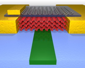 |
| This illustration shows the high performance photodetector which uses few layer black phosphorus (red atoms) to sense light in the waveguide (green material). Graphene (gray atoms) is also used to tune the performance. CREDIT: University of Minnesota, College of Science and Engineering |
Abstract:
Phosphorus, a highly reactive element commonly found in match heads, tracer bullets, and fertilizers, can be turned into a stable crystalline form known as black phosphorus. In a new study, researchers from the University of Minnesota used an ultrathin black phosphorus film--only 20 layers of atoms--to demonstrate high-speed data communication on nanoscale optical circuits.
Black phosphorus is new 'wonder material' for improving optical communication
Minneapolis, MN | Posted on March 3rd, 2015The devices showed vast improvement in efficiency over comparable devices using the earlier "wonder material" graphene.
The work by University of Minnesota Department of Electrical and Computer Engineering Professors Mo Li and Steven Koester and graduate students Nathan Youngblood and Che Chen was published today in Nature Photonics--a leading journal in the field of optics and photonics.
As consumers demand electronic devices that are faster and smaller, electronics makers cram more processor cores on a single chip, but getting all those processors to communicate with each other has been a key challenge for researchers. The goal is to find materials that will allow high-speed, on-chip communication using light.
While the existence of black phosphorus has been known for more than a century, only in the past year has its potential as a semiconductor been realized. Due to its unique properties, black phosphorus can be used to detect light very effectively, making it desirable for optical applications. For the first time, the University of Minnesota team created intricate optical circuits in silicon and then laid thin flakes of black phosphorus over these structures using facilities at the University's Minnesota Nano Center.
"After the discovery of graphene, new two-dimensional materials continue to emerge with novel optoelectronic properties," said Professor Li, who led the research team. "Because these materials are two-dimensional, it makes perfect sense to place them on chips with flat optical integrated circuits to allow maximal interaction with light and optimally utilize their novel properties."
The University of Minnesota team demonstrated that the performance of the black phosphorus photodetectors even rivals that of comparable devices made of germanium--considered the gold standard in on-chip photodetection. Germanium, however, is difficult to grow on silicon optical circuits, while black phosphorus and other two-dimensional materials can be grown separately and transferred onto any material, making them much more versatile.
The team also showed that the devices could be used for real-world applications by sending high-speed optical data over fibers and recovering it using the black phosphorus photodetectors. The group demonstrated data speeds up to three billion bits per second, which is equivalent to downloading a typical HD movie in about 30 seconds.
"Even though we have already demonstrated high speed operation with our devices, we expect higher transfer rates through further optimization," said Nathan Youngblood, the lead author of the study. "Since we are the first to demonstrate a high speed photodetector using black phosphorus, more work still needs to be done to determine the theoretical limits for a fully optimized device."
Bridging the gap
While black phosphorus has much in common with graphene--another two-dimensional material--the materials have significant differences, the most important of which is the existence of an energy gap, often referred to as a "band gap."
Materials with a band gap, known as "semiconductors," are a special group of materials that only conduct electricity when the electrons in that material absorb enough energy for them to "jump" the band gap. This energy can be provided through heat, light, and other means.
While graphene has proven useful for a wide variety of applications, its main limitation is its lack of a band gap. This means that graphene always conducts a significant amount of electricity, and this "leakage" makes graphene devices inefficient. In essence, the device is "on" and leaking electricity all the time.
Black phosphorus, on the other hand, has a widely-tunable band gap that varies depending on how many layers are stacked together. This means that black phosphorus can be tuned to absorb light in the visible range but also in the infrared. This large degree of tunability makes black phosphorus a unique material that can be used for a wide range of applications--from chemical sensing to optical communication.
Additionally, black phosphorus is a so-called "direct-band" semiconductor, meaning it has the potential to efficiently convert electrical signals back into light. Combined with its high performance photodetection abilities, black phosphorus could also be used to generate light in an optical circuit, making it a one-stop solution for on-chip optical communication.
"It is really exciting to think of a single material that can be used to send and receive data optically and is not limited to a specific substrate or wavelength," Youngblood said. "This could have huge potential for high-speed communication between CPU cores which is a bottleneck in computing industry right now."
Fast growing potential
The past several years have seen a flurry of two-dimensional material discoveries, first with graphene, more recently with transition metal dichalcogenides (TMDs) such as molybdenum disulphide (MoS2), and now black phosphorus. All of the previous two-dimensional materials have serious trade offs, but black phosphorus provides the "best of both worlds" with a tunable band gap and high-speed capability.
"Black phosphorus is an extremely versatile material," said Professor Steven Koester, who contributed to the project. "It makes great transistors and photodetectors, and has the potential for light emission and other novel devices, making it an ideal platform for a new type of adaptable electronics technology."
###
The University of Minnesota research was funded by the Air Force Office of Scientific Research and the National Science Foundation.
####
For more information, please click here
Contacts:
Rhonda Zurn
612-626-7959
Copyright © University of Minnesota
If you have a comment, please Contact us.Issuers of news releases, not 7th Wave, Inc. or Nanotechnology Now, are solely responsible for the accuracy of the content.
Bookmark:


| Related News Press |
News and information
![]() Quantum computer improves AI predictions April 17th, 2026
Quantum computer improves AI predictions April 17th, 2026
![]() Flexible sensor gains sensitivity under pressure April 17th, 2026
Flexible sensor gains sensitivity under pressure April 17th, 2026
![]() A reusable chip for particulate matter sensing April 17th, 2026
A reusable chip for particulate matter sensing April 17th, 2026
![]() Detecting vibrational quantum beating in the predissociation dynamics of SF6 using time-resolved photoelectron spectroscopy April 17th, 2026
Detecting vibrational quantum beating in the predissociation dynamics of SF6 using time-resolved photoelectron spectroscopy April 17th, 2026
Graphene/ Graphite
![]() Electrifying results shed light on graphene foam as a potential material for lab grown cartilage June 6th, 2025
Electrifying results shed light on graphene foam as a potential material for lab grown cartilage June 6th, 2025
![]() Breakthrough in proton barrier films using pore-free graphene oxide: Kumamoto University researchers achieve new milestone in advanced coating technologies September 13th, 2024
Breakthrough in proton barrier films using pore-free graphene oxide: Kumamoto University researchers achieve new milestone in advanced coating technologies September 13th, 2024
Govt.-Legislation/Regulation/Funding/Policy
![]() Quantum computer improves AI predictions April 17th, 2026
Quantum computer improves AI predictions April 17th, 2026
![]() Metasurfaces smooth light to boost magnetic sensing precision January 30th, 2026
Metasurfaces smooth light to boost magnetic sensing precision January 30th, 2026
![]() New imaging approach transforms study of bacterial biofilms August 8th, 2025
New imaging approach transforms study of bacterial biofilms August 8th, 2025
Chip Technology
![]() A reusable chip for particulate matter sensing April 17th, 2026
A reusable chip for particulate matter sensing April 17th, 2026
![]() Metasurfaces smooth light to boost magnetic sensing precision January 30th, 2026
Metasurfaces smooth light to boost magnetic sensing precision January 30th, 2026
Optical computing/Photonic computing
![]() ICFO researchers overcome long-standing bottleneck in single photon detection with twisted 2D materials August 8th, 2025
ICFO researchers overcome long-standing bottleneck in single photon detection with twisted 2D materials August 8th, 2025
![]() Programmable electron-induced color router array May 14th, 2025
Programmable electron-induced color router array May 14th, 2025
Discoveries
![]() Quantum computer improves AI predictions April 17th, 2026
Quantum computer improves AI predictions April 17th, 2026
![]() Flexible sensor gains sensitivity under pressure April 17th, 2026
Flexible sensor gains sensitivity under pressure April 17th, 2026
![]() A reusable chip for particulate matter sensing April 17th, 2026
A reusable chip for particulate matter sensing April 17th, 2026
![]() Detecting vibrational quantum beating in the predissociation dynamics of SF6 using time-resolved photoelectron spectroscopy April 17th, 2026
Detecting vibrational quantum beating in the predissociation dynamics of SF6 using time-resolved photoelectron spectroscopy April 17th, 2026
Announcements
![]() A fundamentally new therapeutic approach to cystic fibrosis: Nanobody repairs cellular defect April 17th, 2026
A fundamentally new therapeutic approach to cystic fibrosis: Nanobody repairs cellular defect April 17th, 2026
![]() UC Irvine physicists discover method to reverse �quantum scrambling� : The work addresses the problem of information loss in quantum computing system April 17th, 2026
UC Irvine physicists discover method to reverse �quantum scrambling� : The work addresses the problem of information loss in quantum computing system April 17th, 2026
Interviews/Book Reviews/Essays/Reports/Podcasts/Journals/White papers/Posters
![]() A fundamentally new therapeutic approach to cystic fibrosis: Nanobody repairs cellular defect April 17th, 2026
A fundamentally new therapeutic approach to cystic fibrosis: Nanobody repairs cellular defect April 17th, 2026
![]() UC Irvine physicists discover method to reverse �quantum scrambling� : The work addresses the problem of information loss in quantum computing system April 17th, 2026
UC Irvine physicists discover method to reverse �quantum scrambling� : The work addresses the problem of information loss in quantum computing system April 17th, 2026
Military
![]() Quantum engineers �squeeze� laser frequency combs to make more sensitive gas sensors January 17th, 2025
Quantum engineers �squeeze� laser frequency combs to make more sensitive gas sensors January 17th, 2025
![]() Chainmail-like material could be the future of armor: First 2D mechanically interlocked polymer exhibits exceptional flexibility and strength January 17th, 2025
Chainmail-like material could be the future of armor: First 2D mechanically interlocked polymer exhibits exceptional flexibility and strength January 17th, 2025
![]() Single atoms show their true color July 5th, 2024
Single atoms show their true color July 5th, 2024
![]() NRL charters Navy�s quantum inertial navigation path to reduce drift April 5th, 2024
NRL charters Navy�s quantum inertial navigation path to reduce drift April 5th, 2024
Photonics/Optics/Lasers
![]() Metasurfaces smooth light to boost magnetic sensing precision January 30th, 2026
Metasurfaces smooth light to boost magnetic sensing precision January 30th, 2026
![]() From sensors to smart systems: the rise of AI-driven photonic noses January 30th, 2026
From sensors to smart systems: the rise of AI-driven photonic noses January 30th, 2026
|
|
||
|
|
||
| The latest news from around the world, FREE | ||
|
|
||
|
|
||
| Premium Products | ||
|
|
||
|
Only the news you want to read!
Learn More |
||
|
|
||
|
Full-service, expert consulting
Learn More |
||
|
|
||