Home > Press > UCLA and USC scientists devise breakthrough technique for mapping temperature in tiny electronic devices: Approach could lead to better designs for computer chips
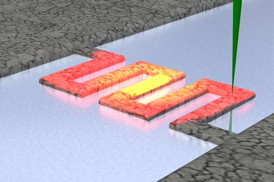 |
| Artist�s conception of plasmon energy expansion thermometry showing a focused electron beam penetrating a 100 nanometer wide aluminum wire atop a thin glass window. The wire�s temperature is mapped by scanning the electron beam. |
Abstract:
Overheating is a major problem for the microprocessors that run our smartphones and computers. But a team of UCLA and USC scientists have made a breakthrough that should enable engineers to design microprocessors that minimize that problem: They have developed a thermal imaging technique that can "see" how the temperature changes from point to point inside the smallest electronic circuits.
UCLA and USC scientists devise breakthrough technique for mapping temperature in tiny electronic devices: Approach could lead to better designs for computer chips
Los Angeles, CA | Posted on February 9th, 2015The technique, called plasmon energy expansion thermometry, or PEET, allows temperatures to be mapped in units as small as a nanometer, a unit of measure equal to one-billionth of a meter. This shatters the previous record for thermal imaging resolution, and it could eventually lead to faster and more capable electronics.
Reported in the February 6 issue of Science, the study reveals � at the atomic level � how heat moves along a tiny aluminum wire that is warmed at one end.
Modern microelectronic circuits contain billions of nanometer-scale transistors. Although each transistor generates only a tiny bit of heat as it operates, with that many transistors operating at once, computer chips get very hot, which is why cellphones get warm and computers need fans to run properly.
To better understand precisely where the heat is being generated, engineers want to be able to map temperature in tiny electronic circuits. Currently, they use one of two thermal imaging techniques: capturing the infrared radiation the device emits or dragging a tiny thermometer back and forth across the device's surface.
But both standard techniques have fundamental limitations. Radiation-based thermometers struggle to resolve devices that are smaller than the wavelengths of the detected radiation, which typically are several thousand nanometers. And bringing a thermometer into contact with a small device generally disturbs the device's temperature. In addition, neither has demonstrated the resolution necessary to "see" the active features in modern transistors, which are typically 22 nanometers across or smaller.
Without a way to measure the temperature of extremely small circuitry, manufacturers have worked blindly, relying on simulations to estimate the devices' temperatures. Now, PEET mapping will enable them to heat a transistor and accurately map which parts of it heat up and track how the heat is transported away � knowledge that could help engineers revolutionize the design of the nanoscale electronics inside the next generation of computing devices.
Led by Chris Regan, a member of UCLA's California NanoSystems Institute and first author Matthew Mecklenburg, a senior staff scientist at USC's Center for Electron Microscopy and Microanalysis, the research team built its technique on the same physical principles behind the glass-bulb thermometer that was invented by Daniel Gabriel Fahrenheit in 1724. Fahrenheit's thermometer gauges temperature from changes in the density of mercury. As mercury is warmed or cooled, it expands or contracts, causing it to move up or down inside a graduated glass cylinder. PEET determines temperature in the same way, by monitoring changes in density. However, UCLA and USC scientists devise breakthrough technique for mapping temperature in tiny electronic devices. PEET determines temperature in the same way, by monitoring changes in density. However, the UCLA- USC team's key advance was to measure changes in the density of the microelectronic device itself rather than using a separate thermometer. In effect, the technique turns the device into its own thermometer.
PEET maps density using a transmission electron microscope. For the Science research, the team demonstrated the technique on tiny aluminum wires that were heated on one end.
They focused the microscope's electron beam to a point, scanned it across the wire and measured the energy of the beam electrons as they came out the other end. Passing through the wire, some of the beam's electrons create charge waves in the wire, called plasmons. Electrons lose energy making those waves, just as a motorboat burns gasoline to make a wake on a pond. Because that energy loss is sensitive to the wire's density, measuring it accurately determines the wire's density, and therefore its temperature; warmer parts of the wire have a slightly lower density. Repeating this measurement thousands of times as they moved the tightly-focused beam over the wire, the team was able to map the wire's temperature with nanometer-scale spatial resolution.
"With the old techniques, measuring the thermal conductivity of a nanowire returns one number. Mapping temperature with PEET, we get 10,000 numbers as we go down the wire. It's the difference between seeing the score and watching the game � one gives you much better knowledge of the players," said Regan, an associate professor of physics and astronomy at UCLA.
According to Mecklenburg, the technique could be adopted easily by electronics manufacturers. "What's especially important is that the transmission electron microscope is already the primary tool used by manufacturers for examining individual microelectronic devices," he said. "We have developed a way to measure thermal gradients with that same microscope � it is a perfect fit. Suddenly, manufacturers can see a new dimension in their devices with the tools they already have."
This research was supported by the National Science Foundation, FAME (a Semiconductor Research Corporation program sponsored by the Microelectronics Advanced Research Corporation and the Defense Advanced Research Projects Agency) and the U.S. Department of Energy.
####
For more information, please click here
Contacts:
Shaun Mason, CNSI
310-794-5346
Copyright © UCLA
If you have a comment, please Contact us.Issuers of news releases, not 7th Wave, Inc. or Nanotechnology Now, are solely responsible for the accuracy of the content.
Bookmark:


| Related News Press |
News and information
![]() Quantum computer improves AI predictions April 17th, 2026
Quantum computer improves AI predictions April 17th, 2026
![]() Flexible sensor gains sensitivity under pressure April 17th, 2026
Flexible sensor gains sensitivity under pressure April 17th, 2026
![]() A reusable chip for particulate matter sensing April 17th, 2026
A reusable chip for particulate matter sensing April 17th, 2026
![]() Detecting vibrational quantum beating in the predissociation dynamics of SF6 using time-resolved photoelectron spectroscopy April 17th, 2026
Detecting vibrational quantum beating in the predissociation dynamics of SF6 using time-resolved photoelectron spectroscopy April 17th, 2026
Govt.-Legislation/Regulation/Funding/Policy
![]() Quantum computer improves AI predictions April 17th, 2026
Quantum computer improves AI predictions April 17th, 2026
![]() Metasurfaces smooth light to boost magnetic sensing precision January 30th, 2026
Metasurfaces smooth light to boost magnetic sensing precision January 30th, 2026
![]() New imaging approach transforms study of bacterial biofilms August 8th, 2025
New imaging approach transforms study of bacterial biofilms August 8th, 2025
Chip Technology
![]() A reusable chip for particulate matter sensing April 17th, 2026
A reusable chip for particulate matter sensing April 17th, 2026
![]() Metasurfaces smooth light to boost magnetic sensing precision January 30th, 2026
Metasurfaces smooth light to boost magnetic sensing precision January 30th, 2026
Discoveries
![]() Quantum computer improves AI predictions April 17th, 2026
Quantum computer improves AI predictions April 17th, 2026
![]() Flexible sensor gains sensitivity under pressure April 17th, 2026
Flexible sensor gains sensitivity under pressure April 17th, 2026
![]() A reusable chip for particulate matter sensing April 17th, 2026
A reusable chip for particulate matter sensing April 17th, 2026
![]() Detecting vibrational quantum beating in the predissociation dynamics of SF6 using time-resolved photoelectron spectroscopy April 17th, 2026
Detecting vibrational quantum beating in the predissociation dynamics of SF6 using time-resolved photoelectron spectroscopy April 17th, 2026
Announcements
![]() A fundamentally new therapeutic approach to cystic fibrosis: Nanobody repairs cellular defect April 17th, 2026
A fundamentally new therapeutic approach to cystic fibrosis: Nanobody repairs cellular defect April 17th, 2026
![]() UC Irvine physicists discover method to reverse �quantum scrambling� : The work addresses the problem of information loss in quantum computing system April 17th, 2026
UC Irvine physicists discover method to reverse �quantum scrambling� : The work addresses the problem of information loss in quantum computing system April 17th, 2026
Military
![]() Quantum engineers �squeeze� laser frequency combs to make more sensitive gas sensors January 17th, 2025
Quantum engineers �squeeze� laser frequency combs to make more sensitive gas sensors January 17th, 2025
![]() Chainmail-like material could be the future of armor: First 2D mechanically interlocked polymer exhibits exceptional flexibility and strength January 17th, 2025
Chainmail-like material could be the future of armor: First 2D mechanically interlocked polymer exhibits exceptional flexibility and strength January 17th, 2025
![]() Single atoms show their true color July 5th, 2024
Single atoms show their true color July 5th, 2024
![]() NRL charters Navy�s quantum inertial navigation path to reduce drift April 5th, 2024
NRL charters Navy�s quantum inertial navigation path to reduce drift April 5th, 2024
Research partnerships
![]() Lab to industry: InSe wafer-scale breakthrough for future electronics August 8th, 2025
Lab to industry: InSe wafer-scale breakthrough for future electronics August 8th, 2025
![]() HKU physicists uncover hidden order in the quantum world through deconfined quantum critical points April 25th, 2025
HKU physicists uncover hidden order in the quantum world through deconfined quantum critical points April 25th, 2025
|
|
||
|
|
||
| The latest news from around the world, FREE | ||
|
|
||
|
|
||
| Premium Products | ||
|
|
||
|
Only the news you want to read!
Learn More |
||
|
|
||
|
Full-service, expert consulting
Learn More |
||
|
|
||