Home > Press > A new dimension for integrated circuits: 3-D nanomagnetic logic: Field-coupled magnets could replace transistors in some computer chips
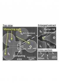 |
| This image shows scanning electron micrographs of a 3-D majority logic gate showing the scale of the computing area ,with dimensions less than 200 nanometers, and, in cross-section, the lower position of the third input magnet.
Credit: I. Eichwald/TUM |
Abstract:
Electrical engineers at the Technische Universität München (TUM) have demonstrated a new kind of building block for digital integrated circuits. Their experiments show that future computer chips could be based on three-dimensional arrangements of nanometer-scale magnets instead of transistors. As the main enabling technology of the semiconductor industry - CMOS fabrication of silicon chips - approaches fundamental limits, the TUM researchers and collaborators at the University of Notre Dame are exploring "magnetic computing" as an alternative. They report their latest results in the journal Nanotechnology.
A new dimension for integrated circuits: 3-D nanomagnetic logic: Field-coupled magnets could replace transistors in some computer chips
Munich, Germany | Posted on October 2nd, 2014In a 3D stack of nanomagnets, the researchers have implemented a so-called majority logic gate, which could serve as a programmable switch in a digital circuit. They explain the underlying principle with a simple illustration: Think of the way ordinary bar magnets behave when you bring them near each other, with opposite poles attracting and like poles repelling each other. Now imagine bringing several bar magnets together and holding all but one in a fixed position. Their magnetic fields can be thought of as being coupled into one, and the "north-south" polarity of the magnet that is free to flip will be determined by the orientation of the majority of fixed magnets.
Gates made from field-coupled nanomagnets work in an analogous way, with the reversal of polarity representing a switch between Boolean logic states, the binary digits 1 and 0. In the 3D majority gate reported by the TUM-Notre Dame team, the state of the device is determined by three input magnets, one of which sits 60 nanometers below the other two, and is read out by a single output magnet.
The Latest in a Line of Advances
This work builds on capabilities the collaborators have developed over several years, ranging from sophisticated simulations of magnetic behavior to innovative fabrication and measuring techniques. It also represents not an end point but a milestone in a series of advances.
For example, they reported the world's first "domain wall gate" at last year's International Electron Devices Meeting. The scientists use focused ion-beam irradation to change the magnetic properties of sharply defined spots on the device. So-called domain walls generated there are able to flow through magnetic wires under the control of surrounding nanomagnets. This 2D device, TUM doctoral candidate Stephan Breitkreutz explains, "enables signal routing, buffering, and synchronization in magnetic circuits, similar to latches in electrical integrated circuits."
A Fork in the Industry Roadmap
All players in the semiconductor business benefit from one industry-wide cooperative effort: developing long-range "roadmaps" that chart potential pathways to common technological goals. In the most recent issue of the International Technology Roadmap for Semiconductors, nanomagnetic logic is given serious consideration among a diverse zoo of "emerging research devices." Magnetic circuits are non-volatile, meaning they don't need power to remember what state they are in. Extremely low energy consumption is one of their most promising characteristics. They also can operate at room temperature and resist radiation.
The potential to pack more gates onto a chip is especially important. Nanomagnetic logic can allow very dense packing, for several reasons. The most basic building blocks, the individual nanomagnets, are comparable in size to individual transistors. Furthermore, where transistors require contacts and wiring, nanomagnets operate purely with coupling fields. Also, in building CMOS and nanomagnetic devices that have the same function - for example, a so-called full-adder - it can take fewer magnets than transistors to get the job done.
Finally, the potential to break out of the 2D design space with stacks of 3D devices makes nanomagnetic logic competitive. TUM doctoral candidate Irina Eichwald, lead author of the Nanotechnology paper, explains: "The 3D majority gate demonstrates that magnetic computing can be exploited in all three dimensions, in order to realize monolithic, sequentially stacked magnetic circuits promising better scalability and improved packing density."
"It is a big challenge to compete with silicon CMOS circuits," adds Dr. Markus Becherer, leader of the TUM research group within the Institute for Technical Electronics. "However, there might be applications where the non-volatile, ultralow-power operation and high integration density offered by 3D nanomagnetic circuits give them an edge."
###
This research was supported by the German Research Foundation (DFG).
Publications
Majority logic gate for 3D magnetic computing, Irina Eichwald, Stephan Breitkreutz, Grazvydas Ziemys, György Csaba, Wolfgang Porod, and Markus Becherer. Nanotechnology, 25 (2014) 335202, doi:10.1088/0957-4484/25/33/335202.
Domain Wall Gate for Magnetic Logic and Memory Applications with Perpendicular Anisotropy, S. Breitkreutz, G. Ziemys, I. Eichwald, J. Kiermaier, G. Csaba, W. Porod, D. Schmitt-Landsiedl, and M. Becherer. IEEE International Electron Devices Meeting (IEDM 2013), pp. 22.4.1-22.4-4, doi:10.1109/IEDM.2013.6724684.
The 2014 Magnetism Roadmap, Robert L. Stamps, Stephan Breitkreutz, et al. J. Phys. D: Appl. Phys. 47 (2014) 333001. doi:10.1088/0022-3727/47/33/333001.
####
About Technische Universitaet Muenchen
Technische Universität München (TUM) is one of Europe's leading research universities, with around 500 professors, 10,000 academic and non-academic staff, and 36,000 students. Its focus areas are the engineering sciences, natural sciences, life sciences and medicine, reinforced by schools of management and education. TUM acts as an entrepreneurial university that promotes talents and creates value for society. In that it profits from having strong partners in science and industry. It is represented worldwide with a campus in Singapore as well as offices in Beijing, Brussels, Cairo, Mumbai, and Săo Paulo. Nobel Prize winners and inventors such as Rudolf Diesel and Carl von Linde have done research at TUM. In 2006 and 2012 it won recognition as a German "Excellence University." In international rankings, it regularly places among the best universities in Germany.
For more information, please click here
Contacts:
Patrick Regan
49-162-427-9876
Irina Eichwald
Institute for Technical Electronics
Technische Universität München
+49 89 289 22923
Stephan Breitkreutz
Institute for Technical Electronics
Technische Universität München
+49 89 289 22348
Markus Becherer
Institute for Technical Electronics
Technische Universität München
+49 89 289 22915
Copyright © Technische Universitaet Muenchen
If you have a comment, please Contact us.Issuers of news releases, not 7th Wave, Inc. or Nanotechnology Now, are solely responsible for the accuracy of the content.
Bookmark:


| Related News Press |
News and information
![]() Quantum computer improves AI predictions April 17th, 2026
Quantum computer improves AI predictions April 17th, 2026
![]() Flexible sensor gains sensitivity under pressure April 17th, 2026
Flexible sensor gains sensitivity under pressure April 17th, 2026
![]() A reusable chip for particulate matter sensing April 17th, 2026
A reusable chip for particulate matter sensing April 17th, 2026
![]() Detecting vibrational quantum beating in the predissociation dynamics of SF6 using time-resolved photoelectron spectroscopy April 17th, 2026
Detecting vibrational quantum beating in the predissociation dynamics of SF6 using time-resolved photoelectron spectroscopy April 17th, 2026
Govt.-Legislation/Regulation/Funding/Policy
![]() Quantum computer improves AI predictions April 17th, 2026
Quantum computer improves AI predictions April 17th, 2026
![]() Metasurfaces smooth light to boost magnetic sensing precision January 30th, 2026
Metasurfaces smooth light to boost magnetic sensing precision January 30th, 2026
![]() New imaging approach transforms study of bacterial biofilms August 8th, 2025
New imaging approach transforms study of bacterial biofilms August 8th, 2025
Chip Technology
![]() A reusable chip for particulate matter sensing April 17th, 2026
A reusable chip for particulate matter sensing April 17th, 2026
![]() Metasurfaces smooth light to boost magnetic sensing precision January 30th, 2026
Metasurfaces smooth light to boost magnetic sensing precision January 30th, 2026
Nanoelectronics
![]() Lab to industry: InSe wafer-scale breakthrough for future electronics August 8th, 2025
Lab to industry: InSe wafer-scale breakthrough for future electronics August 8th, 2025
![]() Interdisciplinary: Rice team tackles the future of semiconductors Multiferroics could be the key to ultralow-energy computing October 6th, 2023
Interdisciplinary: Rice team tackles the future of semiconductors Multiferroics could be the key to ultralow-energy computing October 6th, 2023
![]() Key element for a scalable quantum computer: Physicists from Forschungszentrum Jülich and RWTH Aachen University demonstrate electron transport on a quantum chip September 23rd, 2022
Key element for a scalable quantum computer: Physicists from Forschungszentrum Jülich and RWTH Aachen University demonstrate electron transport on a quantum chip September 23rd, 2022
![]() Reduced power consumption in semiconductor devices September 23rd, 2022
Reduced power consumption in semiconductor devices September 23rd, 2022
Discoveries
![]() Quantum computer improves AI predictions April 17th, 2026
Quantum computer improves AI predictions April 17th, 2026
![]() Flexible sensor gains sensitivity under pressure April 17th, 2026
Flexible sensor gains sensitivity under pressure April 17th, 2026
![]() A reusable chip for particulate matter sensing April 17th, 2026
A reusable chip for particulate matter sensing April 17th, 2026
![]() Detecting vibrational quantum beating in the predissociation dynamics of SF6 using time-resolved photoelectron spectroscopy April 17th, 2026
Detecting vibrational quantum beating in the predissociation dynamics of SF6 using time-resolved photoelectron spectroscopy April 17th, 2026
Announcements
![]() A fundamentally new therapeutic approach to cystic fibrosis: Nanobody repairs cellular defect April 17th, 2026
A fundamentally new therapeutic approach to cystic fibrosis: Nanobody repairs cellular defect April 17th, 2026
![]() UC Irvine physicists discover method to reverse ‘quantum scrambling’ : The work addresses the problem of information loss in quantum computing system April 17th, 2026
UC Irvine physicists discover method to reverse ‘quantum scrambling’ : The work addresses the problem of information loss in quantum computing system April 17th, 2026
Interviews/Book Reviews/Essays/Reports/Podcasts/Journals/White papers/Posters
![]() A fundamentally new therapeutic approach to cystic fibrosis: Nanobody repairs cellular defect April 17th, 2026
A fundamentally new therapeutic approach to cystic fibrosis: Nanobody repairs cellular defect April 17th, 2026
![]() UC Irvine physicists discover method to reverse ‘quantum scrambling’ : The work addresses the problem of information loss in quantum computing system April 17th, 2026
UC Irvine physicists discover method to reverse ‘quantum scrambling’ : The work addresses the problem of information loss in quantum computing system April 17th, 2026
Research partnerships
![]() Lab to industry: InSe wafer-scale breakthrough for future electronics August 8th, 2025
Lab to industry: InSe wafer-scale breakthrough for future electronics August 8th, 2025
![]() HKU physicists uncover hidden order in the quantum world through deconfined quantum critical points April 25th, 2025
HKU physicists uncover hidden order in the quantum world through deconfined quantum critical points April 25th, 2025
|
|
||
|
|
||
| The latest news from around the world, FREE | ||
|
|
||
|
|
||
| Premium Products | ||
|
|
||
|
Only the news you want to read!
Learn More |
||
|
|
||
|
Full-service, expert consulting
Learn More |
||
|
|
||