Home > Press > Penn Study: Understanding Graphene’s Electrical Properties on an Atomic Level
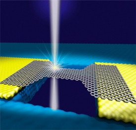 |
| An illustration of a graphene nanoribbon shaped by the beam of a transmission electron microscope. Credit: Robert Johnson |
Abstract:
Graphene, a material that consists of a lattice of carbon atoms, one atom thick, is widely touted as being the most electrically conductive material ever studied. However, not all graphene is the same. With so few atoms comprising the entirety of the material, the arrangement of each one has an impact on its overall function.
Penn Study: Understanding Graphene’s Electrical Properties on an Atomic Level
Philadelphia, PA | Posted on July 22nd, 2014Now, for the first time, researchers from the University of Pennsylvania have used a cutting-edge microscope to study the relationship between the atomic geometry of a ribbon of graphene and its electrical properties.
A deeper understanding of this relationship will be necessary for the design of graphene-based integrated circuits, computer chips and other electronic devices.
The study was led by professors A.T. Charlie Johnson and Marija Drndić, both of the Department of Physics and Astronomy in Penn's School of Arts & Sciences, along with Zhengqing John Qi, a member of Johnson's lab, and Julio Rodríguez-Manzo from Drndic's lab. Sung Ju Hong, then a member of Johnson's lab, also contributed to the study.
The Penn team collaborated with researchers at Brookhaven National Laboratory, the Université Catholique de Louvain in Belgium and Seoul National University in South Korea.
Their study was published in the journal Nano Letters.
The team's experiments were enabled by Brookhaven's aberration-corrected transmission electron microscope, or AC-TEM. By focusing the microscope's electron beam, the researchers were able to controllably cut sheets of graphene into ribbons with widths as small as 10 nanometers, while keeping them connected to an electricity source outside the microscope. They then could use the AC-TEM's nanoscopic resolution to distinguish between individual carbon atoms within those ribbons. This level of precision was necessary to determine how the carbon atoms on the edges of the nanoribbons were oriented.
"We're relating the structure of the graphene — its atomic arrangement — to its electrical transport properties," said Drndić. "In particular, we were looking at the edges, which we were able to identify the geometry of."
"Graphene looks like chicken wire, and you can cut up this hexagonal lattice of carbon atoms in different ways, producing different shapes on the edge," she said. "But if you cut it one way, it might behave more like a metal, and, if you cut it another way, it could be more like a semiconductor."
For any piece of graphene, either the pointy or flat sides of its carbon hexagons might be at the piece's edge. Where the pointy sides face outward, the edge has a "zig-zag" pattern. Flat sides produce "armchair" pattern when they are on an edge. Any given edge might also display a mix of the two, depending on how the piece of graphene was initially cut and how that edge degrades under stress.
Because the graphene nanoribbons were connected to an electricity source while they were inside the AC-TEM, the researchers were able to simultaneously trace the outline of the ribbons and measure their conductivity. This allowed the two figures to be correlated.
"If you want to use graphene nanoribbons in computer chips, for example, you absolutely need to have this information," Johnson said. "People have looked at these ribbons under the microscope, and people have measured their electrical properties without looking at them but never both at the same time."
After studying the nanoribbons with relatively low levels of electron flow, the researchers turned up the intensity, much like turning up a light bulb using a dimmer switch The combination of the electron bombardment from the microscope and the large amount of electrons flowing through the nanoribbons caused their structures to gradually degrade. As carbon bonds within the nanoribbons broke, they became thinner and the shape of their edges changed, providing additional data points.
"By doing everything within the microscope," Rodríguez-Manzo said, "we can just follow this transformation to the end, measuring currents for the nanoribbons even when the get smaller than 1 nanometer across. That's five atoms wide."
This kind of stress testing is critical to the future design of graphene electronics.
"We have to see how much current we can transport before these nanoribbons fall apart. Our data shows that this figure is high compared to copper," Rodríguez-Manzo said.
The harsh conditions also caused some of the ribbons to fold up on themselves, producing nanoscopic graphene loops. Serendipitously, the team found that these loops had desirable properties.
"When the edges wrap around and form the loops we see," Johnson said, "it helps hold the structure together, and it makes the current density a thousand higher than what is currently state of the art. That structure would be useful in making interconnects [which are the conducting paths that connect transistors together in integrated circuits]."
Future research in this field will involve directly comparing the electrical properties of graphene nanoribbons with different widths and edge shapes.
"Once we can cut these nanoribbons atom by atom," Drndić said, "there will be a lot more we can achieve."
The research was supported by the National Science Foundation, the National Institutes of Health, the U.S. Department of Energy, Belgium's Fonds de la Recherche Scientifique, South Korea's Ministry of Education, Science and Technology and National Research Foundation and the European Union's Graphene Flagship Consortium.
Andrés R. Botello-Méndez and Jean-Christophe Charlier of the Université Catholique de Louvain in Belgium, Eric Stach of Brookhaven National Laboratory and Yung Woo Park of Seoul National University also contributed to the study.
####
For more information, please click here
Contacts:
Evan Lerner
215-573-6604
Copyright © University of Pennsylvania
If you have a comment, please Contact us.Issuers of news releases, not 7th Wave, Inc. or Nanotechnology Now, are solely responsible for the accuracy of the content.
Bookmark:


| Related News Press |
News and information
![]() Quantum computer improves AI predictions April 17th, 2026
Quantum computer improves AI predictions April 17th, 2026
![]() Flexible sensor gains sensitivity under pressure April 17th, 2026
Flexible sensor gains sensitivity under pressure April 17th, 2026
![]() A reusable chip for particulate matter sensing April 17th, 2026
A reusable chip for particulate matter sensing April 17th, 2026
![]() Detecting vibrational quantum beating in the predissociation dynamics of SF6 using time-resolved photoelectron spectroscopy April 17th, 2026
Detecting vibrational quantum beating in the predissociation dynamics of SF6 using time-resolved photoelectron spectroscopy April 17th, 2026
Graphene/ Graphite
![]() Electrifying results shed light on graphene foam as a potential material for lab grown cartilage June 6th, 2025
Electrifying results shed light on graphene foam as a potential material for lab grown cartilage June 6th, 2025
![]() Breakthrough in proton barrier films using pore-free graphene oxide: Kumamoto University researchers achieve new milestone in advanced coating technologies September 13th, 2024
Breakthrough in proton barrier films using pore-free graphene oxide: Kumamoto University researchers achieve new milestone in advanced coating technologies September 13th, 2024
Govt.-Legislation/Regulation/Funding/Policy
![]() Quantum computer improves AI predictions April 17th, 2026
Quantum computer improves AI predictions April 17th, 2026
![]() Metasurfaces smooth light to boost magnetic sensing precision January 30th, 2026
Metasurfaces smooth light to boost magnetic sensing precision January 30th, 2026
![]() New imaging approach transforms study of bacterial biofilms August 8th, 2025
New imaging approach transforms study of bacterial biofilms August 8th, 2025
Chip Technology
![]() A reusable chip for particulate matter sensing April 17th, 2026
A reusable chip for particulate matter sensing April 17th, 2026
![]() Metasurfaces smooth light to boost magnetic sensing precision January 30th, 2026
Metasurfaces smooth light to boost magnetic sensing precision January 30th, 2026
Discoveries
![]() Quantum computer improves AI predictions April 17th, 2026
Quantum computer improves AI predictions April 17th, 2026
![]() Flexible sensor gains sensitivity under pressure April 17th, 2026
Flexible sensor gains sensitivity under pressure April 17th, 2026
![]() A reusable chip for particulate matter sensing April 17th, 2026
A reusable chip for particulate matter sensing April 17th, 2026
![]() Detecting vibrational quantum beating in the predissociation dynamics of SF6 using time-resolved photoelectron spectroscopy April 17th, 2026
Detecting vibrational quantum beating in the predissociation dynamics of SF6 using time-resolved photoelectron spectroscopy April 17th, 2026
Materials/Metamaterials/Magnetoresistance
![]() First real-time observation of two-dimensional melting process: Researchers at Mainz University unveil new insights into magnetic vortex structures August 8th, 2025
First real-time observation of two-dimensional melting process: Researchers at Mainz University unveil new insights into magnetic vortex structures August 8th, 2025
![]() Researchers unveil a groundbreaking clay-based solution to capture carbon dioxide and combat climate change June 6th, 2025
Researchers unveil a groundbreaking clay-based solution to capture carbon dioxide and combat climate change June 6th, 2025
![]() A 1960s idea inspires NBI researchers to study hitherto inaccessible quantum states June 6th, 2025
A 1960s idea inspires NBI researchers to study hitherto inaccessible quantum states June 6th, 2025
![]() Institute for Nanoscience hosts annual proposal planning meeting May 16th, 2025
Institute for Nanoscience hosts annual proposal planning meeting May 16th, 2025
Announcements
![]() A fundamentally new therapeutic approach to cystic fibrosis: Nanobody repairs cellular defect April 17th, 2026
A fundamentally new therapeutic approach to cystic fibrosis: Nanobody repairs cellular defect April 17th, 2026
![]() UC Irvine physicists discover method to reverse ‘quantum scrambling’ : The work addresses the problem of information loss in quantum computing system April 17th, 2026
UC Irvine physicists discover method to reverse ‘quantum scrambling’ : The work addresses the problem of information loss in quantum computing system April 17th, 2026
Interviews/Book Reviews/Essays/Reports/Podcasts/Journals/White papers/Posters
![]() A fundamentally new therapeutic approach to cystic fibrosis: Nanobody repairs cellular defect April 17th, 2026
A fundamentally new therapeutic approach to cystic fibrosis: Nanobody repairs cellular defect April 17th, 2026
![]() UC Irvine physicists discover method to reverse ‘quantum scrambling’ : The work addresses the problem of information loss in quantum computing system April 17th, 2026
UC Irvine physicists discover method to reverse ‘quantum scrambling’ : The work addresses the problem of information loss in quantum computing system April 17th, 2026
Research partnerships
![]() Lab to industry: InSe wafer-scale breakthrough for future electronics August 8th, 2025
Lab to industry: InSe wafer-scale breakthrough for future electronics August 8th, 2025
![]() HKU physicists uncover hidden order in the quantum world through deconfined quantum critical points April 25th, 2025
HKU physicists uncover hidden order in the quantum world through deconfined quantum critical points April 25th, 2025
|
|
||
|
|
||
| The latest news from around the world, FREE | ||
|
|
||
|
|
||
| Premium Products | ||
|
|
||
|
Only the news you want to read!
Learn More |
||
|
|
||
|
Full-service, expert consulting
Learn More |
||
|
|
||