Home > Press > Bruker Introduces Inspire Nanoscale Chemical Mapping System: Featuring New PeakForce IR SPM Mode for Comprehensive Nanocharacterization
 |
Abstract:
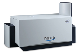
Bruker (NASDAQ: BRKR) today announced the release of Inspire™, the first integrated scanning probe microscopy (SPM) infrared system for 10-nanometer spatial resolution in chemical and materials property mapping. The new and unique Inspire system incorporates Bruker's proprietary PeakForce IR™ mode to enable nanoscale infrared reflection and absorption mapping for a wide range of applications, including the characterization of microphases and their interfaces in polymer blends, plasmons in the two-dimensional electron gas of graphene, and chemical heterogeneity in complex materials and thin films.
Bruker Introduces Inspire Nanoscale Chemical Mapping System: Featuring New PeakForce IR SPM Mode for Comprehensive Nanocharacterization
Billerica, MA | Posted on July 10th, 2014The Inspire system features sensitivity down to molecular monolayers, even on samples not amenable to standard atomic force microscopy techniques. Inspire utilizes fully integrated infrared scattering, scanning near-field optical microscope (SNOM) optics, point-and-click alignment, and the full suite of exclusive PeakForce Tapping® technologies found on Bruker's performance-leading AFMs, from ScanAsyst® self-optimization to quantitative PeakForce QNM® nanomechanics and PeakForce KPFM™ work function measurements. The resulting Inspire solution now provides instant access to the highest resolution chemical, plasmonics, nanomechanical, and electrical characterization for new scientific research and nano-analytical frontiers.
"The infrared scattering SNOM technique has great potential for new scientific discoveries through highest resolution spatio-spectral imaging," explained Professor Markus B. Raschke, Departments of Physics and Chemistry, and JILA, at the University of Colorado, Boulder. "Its wide, productive application has been held back by the lack of an integrated solution."
"With Inspire, we now have provided this integrated solution, which is a major milestone on our path to enable even more widespread AFM adoption by providing new, nanoscale chemical information to researchers," added David V. Rossi, Executive Vice President and General Manager of Bruker's AFM Business. "Inspire builds upon our exclusive PeakForce Tapping technology to provide a complete set of the highest resolution nanochemical and nanomechanical property maps together with topography in a single SPM measurement.""
####
About Bruker Corporation
Bruker Corporation is a leading provider of high-performance scientific instruments and solutions for molecular, cellular and materials research, as well as for industrial, diagnostics, clinical research and applied analysis.
About Inspire
Inspire is a scanning probe based nanoscale characterization system that extends atomic force microscopy into the chemical regime by providing infrared absorption and reflection imaging down to a spatial resolution of 10 nanometers utilizing scattering scanning near-field optical microscopy (SNOM). Inspire includes all optics, detectors and configurable sources, as well as all AFM hardware and software for atomic resolution imaging in a compact and robust integrated package. Inspire also comes with Bruker’s new PeakForce IR mode, which builds on Bruker’s exclusive PeakForce Tapping direct force control technology. PeakForce IR overcomes the limitations of contact and of TappingMode™, and thus of traditional near-field optical and photothermal approaches to nanoscale infrared imaging. It also avoids sample damage from lateral forces, retaining highest resolution on soft polymers, and enables high-resolution imaging of polymer brushes and even powders. PeakForce IR includes ScanAsyst self-optimization and PeakForce QNM for instantly correlated nanomechanical data. The comprehensive set of optional modes includes PeakForce TUNA™, which enables conductivity mapping on samples not amenable to contact mode AFM, and PeakForce KPFM, which employs FM detection for the highest spatial resolution work function mapping while avoiding the mechanical cross-talk affecting single-pass FM-KPFM.
For more information, please click here
Contacts:
Stephen Hopkins, Marketing Communications
Bruker Nano Surfaces Division
3400 East Britannia Drive, Suite 150, Tucson, AZ 85706
T: +1 (520) 741-1044 x1022
Copyright © Bruker Corporation
If you have a comment, please Contact us.Issuers of news releases, not 7th Wave, Inc. or Nanotechnology Now, are solely responsible for the accuracy of the content.
Bookmark:


| Related News Press |
News and information
![]() Quantum computer improves AI predictions April 17th, 2026
Quantum computer improves AI predictions April 17th, 2026
![]() Flexible sensor gains sensitivity under pressure April 17th, 2026
Flexible sensor gains sensitivity under pressure April 17th, 2026
![]() A reusable chip for particulate matter sensing April 17th, 2026
A reusable chip for particulate matter sensing April 17th, 2026
![]() Detecting vibrational quantum beating in the predissociation dynamics of SF6 using time-resolved photoelectron spectroscopy April 17th, 2026
Detecting vibrational quantum beating in the predissociation dynamics of SF6 using time-resolved photoelectron spectroscopy April 17th, 2026
Imaging
![]() Simple algorithm paired with standard imaging tool could predict failure in lithium metal batteries August 8th, 2025
Simple algorithm paired with standard imaging tool could predict failure in lithium metal batteries August 8th, 2025
Announcements
![]() A fundamentally new therapeutic approach to cystic fibrosis: Nanobody repairs cellular defect April 17th, 2026
A fundamentally new therapeutic approach to cystic fibrosis: Nanobody repairs cellular defect April 17th, 2026
![]() UC Irvine physicists discover method to reverse ‘quantum scrambling’ : The work addresses the problem of information loss in quantum computing system April 17th, 2026
UC Irvine physicists discover method to reverse ‘quantum scrambling’ : The work addresses the problem of information loss in quantum computing system April 17th, 2026
Tools
![]() Metasurfaces smooth light to boost magnetic sensing precision January 30th, 2026
Metasurfaces smooth light to boost magnetic sensing precision January 30th, 2026
![]() From sensors to smart systems: the rise of AI-driven photonic noses January 30th, 2026
From sensors to smart systems: the rise of AI-driven photonic noses January 30th, 2026
![]() Japan launches fully domestically produced quantum computer: Expo visitors to experience quantum computing firsthand August 8th, 2025
Japan launches fully domestically produced quantum computer: Expo visitors to experience quantum computing firsthand August 8th, 2025
|
|
||
|
|
||
| The latest news from around the world, FREE | ||
|
|
||
|
|
||
| Premium Products | ||
|
|
||
|
Only the news you want to read!
Learn More |
||
|
|
||
|
Full-service, expert consulting
Learn More |
||
|
|
||