Home > Press > Toyohashi Tech researchers have developed a simple, low-loss waveguide for Surface Plasmon Polaritons (SPPs) that is applicable to nanoscale photonic integrated circuits on silicon
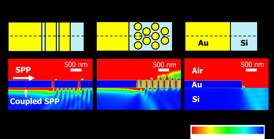 |
| Schematic diagrams and electric field intensity distributions for (a) a multi-slit structure, (b) a disk array, and (c) no diffraction structure at the waveguide end. |
Abstract:
Surface plasmon polaritons (SPPs) are waves that propagate along the surface of a conductor and collective oscillation of electrons coupled with the optical field at the nano-scale beyond the diffraction limit of propagating light waves. Recently, there is increasing interest in SPPs as signal carriers in nanoscale integrated circuits to increase the degree of accumulation and reduce power consumption.
However, low-loss SPP waveguides with detectors have not been developed for applying to nanoscale integrated circuits.
Toyohashi Tech researchers have developed a simple, low-loss waveguide for Surface Plasmon Polaritons (SPPs) that is applicable to nanoscale photonic integrated circuits on silicon
Toyohashi, Japan | Posted on June 24th, 2014Now, Mitsuo Fukuda and his group at Toyohashi Tech have developed a simple, low-loss waveguide for SPPs that is applicable to nanoscale integrated circuits.
A thin metal film deposited on a silicon substrate was terminated with a diffraction structure (a multi-slit or a metal disk array) at the end to guide the SPPs transmitted on the surface (air-metal interface) to the opposite side of the metal (metal-silicon interface). A Schottky barrier is formed at the metal-silicon interface, and the free electrons in the metal are excited by the guided SPPs and then cross over the barrier. The overflowing electrons result in observable photocurrents.
The waveguide developed in this research enabled the efficient propagation of SSPs in 1550-nm-wavelength bands (transparent to silicon) along the Au film surface, and the photocurrents were much larger than for waveguides without the diffraction structure (26 times for the grating structure and 10 times for the disk array).
This waveguide device is expected to contribute to nanoscale photonic integrated circuits on silicon.
Reference:
Authors: M. Fukuhara, M. Ota, H. Sakai, T. Aihara, Y. Ishii, and M. Fukuda.
Title of original paper: Low-loss waveguiding and detecting structure for surface plasmon polaritons.
Journal, volume, pages and year: Applied Physics Letters, 104, 081111 (2014).
Digital Object Identifier (DOI): 10.1063/1.4866792
Affiliations: Department of Electrical & Electronic information Engineering.
Website: www.photon.ee.tut.ac.jp
####
About Toyohashi University of Technology
Founded in 1976, Toyohashi University of Technology is a vibrant modern institute with research activities reflecting the modern era of advanced electronics, engineering, and life sciences.
For more information, please click here
Contacts:
Toyohashi University of Technology
1-1 Hibarigaoka, Tempaku
Toyohashi, Aichi Prefecture, 441-8580, JAPAN
Inquiries: Committee for Public Relations
Copyright © Toyohashi University of Technology
If you have a comment, please Contact us.Issuers of news releases, not 7th Wave, Inc. or Nanotechnology Now, are solely responsible for the accuracy of the content.
Bookmark:


| Related News Press |
News and information
![]() Quantum computer improves AI predictions April 17th, 2026
Quantum computer improves AI predictions April 17th, 2026
![]() Flexible sensor gains sensitivity under pressure April 17th, 2026
Flexible sensor gains sensitivity under pressure April 17th, 2026
![]() A reusable chip for particulate matter sensing April 17th, 2026
A reusable chip for particulate matter sensing April 17th, 2026
![]() Detecting vibrational quantum beating in the predissociation dynamics of SF6 using time-resolved photoelectron spectroscopy April 17th, 2026
Detecting vibrational quantum beating in the predissociation dynamics of SF6 using time-resolved photoelectron spectroscopy April 17th, 2026
Physics
![]() UC Irvine physicists discover method to reverse �quantum scrambling� : The work addresses the problem of information loss in quantum computing system April 17th, 2026
UC Irvine physicists discover method to reverse �quantum scrambling� : The work addresses the problem of information loss in quantum computing system April 17th, 2026
![]() Quantum computers simulate fundamental physics: shedding light on the building blocks of nature June 6th, 2025
Quantum computers simulate fundamental physics: shedding light on the building blocks of nature June 6th, 2025
Chip Technology
![]() A reusable chip for particulate matter sensing April 17th, 2026
A reusable chip for particulate matter sensing April 17th, 2026
![]() Metasurfaces smooth light to boost magnetic sensing precision January 30th, 2026
Metasurfaces smooth light to boost magnetic sensing precision January 30th, 2026
Discoveries
![]() Quantum computer improves AI predictions April 17th, 2026
Quantum computer improves AI predictions April 17th, 2026
![]() Flexible sensor gains sensitivity under pressure April 17th, 2026
Flexible sensor gains sensitivity under pressure April 17th, 2026
![]() A reusable chip for particulate matter sensing April 17th, 2026
A reusable chip for particulate matter sensing April 17th, 2026
![]() Detecting vibrational quantum beating in the predissociation dynamics of SF6 using time-resolved photoelectron spectroscopy April 17th, 2026
Detecting vibrational quantum beating in the predissociation dynamics of SF6 using time-resolved photoelectron spectroscopy April 17th, 2026
Announcements
![]() A fundamentally new therapeutic approach to cystic fibrosis: Nanobody repairs cellular defect April 17th, 2026
A fundamentally new therapeutic approach to cystic fibrosis: Nanobody repairs cellular defect April 17th, 2026
![]() UC Irvine physicists discover method to reverse �quantum scrambling� : The work addresses the problem of information loss in quantum computing system April 17th, 2026
UC Irvine physicists discover method to reverse �quantum scrambling� : The work addresses the problem of information loss in quantum computing system April 17th, 2026
Interviews/Book Reviews/Essays/Reports/Podcasts/Journals/White papers/Posters
![]() A fundamentally new therapeutic approach to cystic fibrosis: Nanobody repairs cellular defect April 17th, 2026
A fundamentally new therapeutic approach to cystic fibrosis: Nanobody repairs cellular defect April 17th, 2026
![]() UC Irvine physicists discover method to reverse �quantum scrambling� : The work addresses the problem of information loss in quantum computing system April 17th, 2026
UC Irvine physicists discover method to reverse �quantum scrambling� : The work addresses the problem of information loss in quantum computing system April 17th, 2026
Photonics/Optics/Lasers
![]() Metasurfaces smooth light to boost magnetic sensing precision January 30th, 2026
Metasurfaces smooth light to boost magnetic sensing precision January 30th, 2026
![]() From sensors to smart systems: the rise of AI-driven photonic noses January 30th, 2026
From sensors to smart systems: the rise of AI-driven photonic noses January 30th, 2026
|
|
||
|
|
||
| The latest news from around the world, FREE | ||
|
|
||
|
|
||
| Premium Products | ||
|
|
||
|
Only the news you want to read!
Learn More |
||
|
|
||
|
Full-service, expert consulting
Learn More |
||
|
|
||