Home > Press > 2D Transistors Promise a Faster Electronics Future Berkeley Lab Researchers Create the First Fully 2D Field Effect Transistors
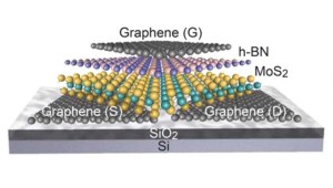 |
| Berkeley Lab researchers fabricated the first fully 2D field-effect transistor from layers of molybdenum disulfide, hexagonal boron nitride and graphene held together by van der Waals bonding. |
Abstract:
Faster electronic device architectures are in the offing with the unveiling of the world's first fully two-dimensional field-effect transistor (FET) by researchers with the Lawrence Berkeley National Laboratory (Berkeley Lab). Unlike conventional FETs made from silicon, these 2D FETs suffer no performance drop-off under high voltages and provide high electron mobility, even when scaled to a monolayer in thickness.
2D Transistors Promise a Faster Electronics Future Berkeley Lab Researchers Create the First Fully 2D Field Effect Transistors
Berkeley, CA | Posted on June 3rd, 2014Ali Javey, a faculty scientist in Berkeley Lab's Materials Sciences Division and a UC Berkeley professor of electrical engineering and computer science, led this research in which 2D heterostructures were fabricated from layers of a transition metal dichalcogenide, hexagonal boron nitride and graphene stacked via van der Waals interactions.
"Our work represents an important stepping stone towards the realization of a new class of electronic devices in which interfaces based on van der Waals interactions rather than covalent bonding provide an unprecedented degree of control in material engineering and device exploration," Javey says. "The results demonstrate the promise of using an all-layered material system for future electronic applications."
Javey is the corresponding author of a paper describing this research in ACS Nano titled "Field-Effect Transistors Built from All Two-Dimensional Material Components". Co-authors are Tania Roy, Mahmut Tosun, Jeong Seuk Kang, Angada Sachid, Sujay Desai, Mark Hettick and Chenming Hu.
FETs, so-called because an electrical signal sent through one electrode creates an electrical current throughout the device, are one of the pillars of the electronics industry, ubiquitous to computers, cell phones, tablets, pads and virtually every other widely used electronic device. All FETs are comprised of gate, source and drain electrodes connected by a channel through which a charge-carrier - either electrons or holes - flow. Mismatches between the crystal structure and atomic lattices of these individual components result in rough surfaces - often with dangling chemical bonds - that degrade charge-carrier mobility, especially at high electrical fields.
"In constructing our 2D FETs so that each component is made from layered materials with van der Waals interfaces, we provide a unique device structure in which the thickness of each component is well-defined without any surface roughness, not even at the atomic level," Javey says. "The van der Waals bonding of the interfaces and the use of a multi-step transfer process present a platform for making complex devices based on crystalline layers without the constraints of lattice parameters that often limit the growth and performance of conventional heterojunction materials."
Javey and his team fabricated their 2D FETs using the transition metal dichalcogenide molybdenum disulfide as the electron-carrying channel, hexagonal boron nitride as the gate insulator, and graphene as the source, drain and gate electrodes. All of these constituent materials are single crystals held together by van der Waals bonding.
For the 2D FETs produced in this study, mechanical exfoliation was used to create the layered components. In the future, Javey and his team will look into growing these heterogeneous layers directly on a substrate. They will also look to scale down the thickness of individual components to a monolayer and the lengths of the channels to molecular-scale dimensions.
This research was funded by the U.S. Department of Energy's Office of Science.
####
For more information, please click here
Contacts:
Lynn Yarris
510-486-5375
Copyright © DOE/Lawrence Berkeley National Laboratory
If you have a comment, please Contact us.Issuers of news releases, not 7th Wave, Inc. or Nanotechnology Now, are solely responsible for the accuracy of the content.
Bookmark:


| Related Links |
![]() For more about the research of Ali Javey and his group go here:
For more about the research of Ali Javey and his group go here:
| Related News Press |
Laboratories
![]() Researchers develop molecular qubits that communicate at telecom frequencies October 3rd, 2025
Researchers develop molecular qubits that communicate at telecom frequencies October 3rd, 2025
Graphene/ Graphite
![]() Electrifying results shed light on graphene foam as a potential material for lab grown cartilage June 6th, 2025
Electrifying results shed light on graphene foam as a potential material for lab grown cartilage June 6th, 2025
![]() Breakthrough in proton barrier films using pore-free graphene oxide: Kumamoto University researchers achieve new milestone in advanced coating technologies September 13th, 2024
Breakthrough in proton barrier films using pore-free graphene oxide: Kumamoto University researchers achieve new milestone in advanced coating technologies September 13th, 2024
Govt.-Legislation/Regulation/Funding/Policy
![]() Quantum computer improves AI predictions April 17th, 2026
Quantum computer improves AI predictions April 17th, 2026
![]() Metasurfaces smooth light to boost magnetic sensing precision January 30th, 2026
Metasurfaces smooth light to boost magnetic sensing precision January 30th, 2026
![]() New imaging approach transforms study of bacterial biofilms August 8th, 2025
New imaging approach transforms study of bacterial biofilms August 8th, 2025
Chip Technology
![]() A reusable chip for particulate matter sensing April 17th, 2026
A reusable chip for particulate matter sensing April 17th, 2026
![]() Metasurfaces smooth light to boost magnetic sensing precision January 30th, 2026
Metasurfaces smooth light to boost magnetic sensing precision January 30th, 2026
Discoveries
![]() Quantum computer improves AI predictions April 17th, 2026
Quantum computer improves AI predictions April 17th, 2026
![]() Flexible sensor gains sensitivity under pressure April 17th, 2026
Flexible sensor gains sensitivity under pressure April 17th, 2026
![]() A reusable chip for particulate matter sensing April 17th, 2026
A reusable chip for particulate matter sensing April 17th, 2026
![]() Detecting vibrational quantum beating in the predissociation dynamics of SF6 using time-resolved photoelectron spectroscopy April 17th, 2026
Detecting vibrational quantum beating in the predissociation dynamics of SF6 using time-resolved photoelectron spectroscopy April 17th, 2026
Materials/Metamaterials/Magnetoresistance
![]() First real-time observation of two-dimensional melting process: Researchers at Mainz University unveil new insights into magnetic vortex structures August 8th, 2025
First real-time observation of two-dimensional melting process: Researchers at Mainz University unveil new insights into magnetic vortex structures August 8th, 2025
![]() Researchers unveil a groundbreaking clay-based solution to capture carbon dioxide and combat climate change June 6th, 2025
Researchers unveil a groundbreaking clay-based solution to capture carbon dioxide and combat climate change June 6th, 2025
![]() A 1960s idea inspires NBI researchers to study hitherto inaccessible quantum states June 6th, 2025
A 1960s idea inspires NBI researchers to study hitherto inaccessible quantum states June 6th, 2025
![]() Institute for Nanoscience hosts annual proposal planning meeting May 16th, 2025
Institute for Nanoscience hosts annual proposal planning meeting May 16th, 2025
Announcements
![]() A fundamentally new therapeutic approach to cystic fibrosis: Nanobody repairs cellular defect April 17th, 2026
A fundamentally new therapeutic approach to cystic fibrosis: Nanobody repairs cellular defect April 17th, 2026
![]() UC Irvine physicists discover method to reverse �quantum scrambling� : The work addresses the problem of information loss in quantum computing system April 17th, 2026
UC Irvine physicists discover method to reverse �quantum scrambling� : The work addresses the problem of information loss in quantum computing system April 17th, 2026
Interviews/Book Reviews/Essays/Reports/Podcasts/Journals/White papers/Posters
![]() A fundamentally new therapeutic approach to cystic fibrosis: Nanobody repairs cellular defect April 17th, 2026
A fundamentally new therapeutic approach to cystic fibrosis: Nanobody repairs cellular defect April 17th, 2026
![]() UC Irvine physicists discover method to reverse �quantum scrambling� : The work addresses the problem of information loss in quantum computing system April 17th, 2026
UC Irvine physicists discover method to reverse �quantum scrambling� : The work addresses the problem of information loss in quantum computing system April 17th, 2026
|
|
||
|
|
||
| The latest news from around the world, FREE | ||
|
|
||
|
|
||
| Premium Products | ||
|
|
||
|
Only the news you want to read!
Learn More |
||
|
|
||
|
Full-service, expert consulting
Learn More |
||
|
|
||