Home > Press > Lighting the Way to Graphene-based Devices: Berkeley Lab Researchers Use Light to Dope Graphene Boron Nitride Heterostructures
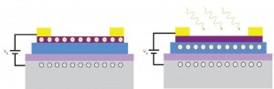 |
| Semiconductors made from graphene and boron nitride can be charge-doped using light. When the GBN heterostructure is exposed to light (green arrows), positive charges move from the graphene layer (purple) to boron nitride layer (blue). |
Abstract:
Graphene continues to reign as the next potential superstar material for the electronics industry, a slimmer, stronger and much faster electron conductor than silicon. With no natural energy band-gap, however, graphene's superfast conductance can't be switched off, a serious drawback for transistors and other electronic devices. Various techniques have been deployed to overcome this problem with one of the most promising being the integration of ultrathin layers of graphene and boron nitride into two-dimensional heterostructures. As conductors, these bilayered hybrids are almost as fast as pure graphene, plus they are well-suited for making devices. However, tailoring the electronic properties of graphene boron nitride (GBN) heterostructures has been a tricky affair, involving chemical doping or electrostatic-gating - until now.
Lighting the Way to Graphene-based Devices: Berkeley Lab Researchers Use Light to Dope Graphene Boron Nitride Heterostructures
Berkeley, CA | Posted on May 18th, 2014Researchers with Berkeley Lab and the University of California (UC) Berkeley have demonstrated a technique whereby the electronic properties of GBN heterostructures can be modified with visible light. Feng Wang, a condensed matter physicist with Berkeley Lab's Materials Sciences Division and UC Berkeley's Physics Department, as well as an investigator for the Kavli Energy NanoSciences Institute at Berkeley, led a study in which photo-induced doping of GBN heterostructures was used to create p-n junctions and other useful doping profiles while preserving the material's remarkably high electron mobility.
"We've demonstrated that visible light can induce a robust writing and erasing of charge-doping in GBN heterostructures without sacrificing high carrier mobility," Wang says. "The use of visible light gives us incredible flexibility and, unlike electrostatic gating and chemical doping, does not require multi-step fabrication processes that reduce sample quality. Additionally, different patterns can be imparted and erased at will, which was not possible with doping techniques previously used on GBN heterostructures."
Graphene is a single layer of carbon atoms arranged in a hexagonal lattice. Boron nitride is a layered compound that features a similar hexagonal lattice - in fact hexagonal boron nitride is sometimes referred to as "white graphene." Bound together by the relatively weak intermolecular attraction known as the van der Waals force, GBN heterostructures have shown high potential to serve as platforms not only for high-electron-mobility transistors, but also for optoelectronic applications, including photodetectors and photovoltaic cells. The key to future success will be the ability to dope these materials in a commercially scalable manner. The photo-induced modulation doping technique developed by Wang and a large team of collaborators meets this requirement as it is comparable to the photolithography schemes widely used today for mass production in the semiconductor industry. Illumination of a GBN heterostructure even with just an incandescent lamp can modify electron-transport in the graphene layer by inducing a positive-charge distribution in the boron nitride layer that becomes fixed when the illumination is turned off.
"We've shown show that this photo-induced doping arises from microscopically coupled optical and electrical responses in the GBN heterostructures, including optical excitation of defect transitions in boron nitride, electrical transport in graphene, and charge transfer between boron nitride and graphene," Wang says. "This is analogous to the modulation doping first developed for high-quality semiconductors."
While the photo-induced modulation doping of GBN heterostructures only lasted a few days if the sample was kept in darkness - further exposure to light erased the effect - this is not a concern as Wang explains.
"A few days of modulation doping are sufficient for many avenues of scientific inquiry, and for some device applications, the rewritability we can provide is needed more than long term stability," he says. "For the moment, what we have is a simple technique for inhomogeneous doping in a high-mobility graphene material that opens the door to novel scientific studies and applications."
A paper on this research has been published in the journal Nature Nanotechnology entitled "Photoinduced doping in heterostructures of graphene and boron nitride." Co-authors are Long Ju, Jairo Velasco Jr., Edwin Huang, Salman Kahn, Casey Nosiglia, Hsin-Zon Tsai, Wei Yang, Takashi Taniguchi, Kenji Watanabe, Yuanbo Zhang, Guangyu Zhang, Michael Crommie and Alex Zettl.
This research was supported by the U.S. Department of Energy's Office of Science and the Office of Naval Research.
####
For more information, please click here
Contacts:
Lynn Yarris
510-486-5375
Copyright © DOE/Lawrence Berkeley National Laboratory
If you have a comment, please Contact us.Issuers of news releases, not 7th Wave, Inc. or Nanotechnology Now, are solely responsible for the accuracy of the content.
Bookmark:


| Related Links |
![]() For more about the research of Feng Wang go here:
For more about the research of Feng Wang go here:
| Related News Press |
News and information
![]() Quantum computer improves AI predictions April 17th, 2026
Quantum computer improves AI predictions April 17th, 2026
![]() Flexible sensor gains sensitivity under pressure April 17th, 2026
Flexible sensor gains sensitivity under pressure April 17th, 2026
![]() A reusable chip for particulate matter sensing April 17th, 2026
A reusable chip for particulate matter sensing April 17th, 2026
![]() Detecting vibrational quantum beating in the predissociation dynamics of SF6 using time-resolved photoelectron spectroscopy April 17th, 2026
Detecting vibrational quantum beating in the predissociation dynamics of SF6 using time-resolved photoelectron spectroscopy April 17th, 2026
Physics
![]() UC Irvine physicists discover method to reverse �quantum scrambling� : The work addresses the problem of information loss in quantum computing system April 17th, 2026
UC Irvine physicists discover method to reverse �quantum scrambling� : The work addresses the problem of information loss in quantum computing system April 17th, 2026
![]() Quantum computers simulate fundamental physics: shedding light on the building blocks of nature June 6th, 2025
Quantum computers simulate fundamental physics: shedding light on the building blocks of nature June 6th, 2025
![]() A 1960s idea inspires NBI researchers to study hitherto inaccessible quantum states June 6th, 2025
A 1960s idea inspires NBI researchers to study hitherto inaccessible quantum states June 6th, 2025
![]() Magnetism in new exotic material opens the way for robust quantum computers June 4th, 2025
Magnetism in new exotic material opens the way for robust quantum computers June 4th, 2025
Laboratories
![]() Researchers develop molecular qubits that communicate at telecom frequencies October 3rd, 2025
Researchers develop molecular qubits that communicate at telecom frequencies October 3rd, 2025
Graphene/ Graphite
![]() Electrifying results shed light on graphene foam as a potential material for lab grown cartilage June 6th, 2025
Electrifying results shed light on graphene foam as a potential material for lab grown cartilage June 6th, 2025
Govt.-Legislation/Regulation/Funding/Policy
![]() Quantum computer improves AI predictions April 17th, 2026
Quantum computer improves AI predictions April 17th, 2026
![]() Metasurfaces smooth light to boost magnetic sensing precision January 30th, 2026
Metasurfaces smooth light to boost magnetic sensing precision January 30th, 2026
![]() New imaging approach transforms study of bacterial biofilms August 8th, 2025
New imaging approach transforms study of bacterial biofilms August 8th, 2025
Chip Technology
![]() A reusable chip for particulate matter sensing April 17th, 2026
A reusable chip for particulate matter sensing April 17th, 2026
![]() Metasurfaces smooth light to boost magnetic sensing precision January 30th, 2026
Metasurfaces smooth light to boost magnetic sensing precision January 30th, 2026
Discoveries
![]() Quantum computer improves AI predictions April 17th, 2026
Quantum computer improves AI predictions April 17th, 2026
![]() Flexible sensor gains sensitivity under pressure April 17th, 2026
Flexible sensor gains sensitivity under pressure April 17th, 2026
![]() A reusable chip for particulate matter sensing April 17th, 2026
A reusable chip for particulate matter sensing April 17th, 2026
![]() Detecting vibrational quantum beating in the predissociation dynamics of SF6 using time-resolved photoelectron spectroscopy April 17th, 2026
Detecting vibrational quantum beating in the predissociation dynamics of SF6 using time-resolved photoelectron spectroscopy April 17th, 2026
Announcements
![]() A fundamentally new therapeutic approach to cystic fibrosis: Nanobody repairs cellular defect April 17th, 2026
A fundamentally new therapeutic approach to cystic fibrosis: Nanobody repairs cellular defect April 17th, 2026
![]() UC Irvine physicists discover method to reverse �quantum scrambling� : The work addresses the problem of information loss in quantum computing system April 17th, 2026
UC Irvine physicists discover method to reverse �quantum scrambling� : The work addresses the problem of information loss in quantum computing system April 17th, 2026
Interviews/Book Reviews/Essays/Reports/Podcasts/Journals/White papers/Posters
![]() A fundamentally new therapeutic approach to cystic fibrosis: Nanobody repairs cellular defect April 17th, 2026
A fundamentally new therapeutic approach to cystic fibrosis: Nanobody repairs cellular defect April 17th, 2026
![]() UC Irvine physicists discover method to reverse �quantum scrambling� : The work addresses the problem of information loss in quantum computing system April 17th, 2026
UC Irvine physicists discover method to reverse �quantum scrambling� : The work addresses the problem of information loss in quantum computing system April 17th, 2026
Military
![]() Quantum engineers �squeeze� laser frequency combs to make more sensitive gas sensors January 17th, 2025
Quantum engineers �squeeze� laser frequency combs to make more sensitive gas sensors January 17th, 2025
![]() Chainmail-like material could be the future of armor: First 2D mechanically interlocked polymer exhibits exceptional flexibility and strength January 17th, 2025
Chainmail-like material could be the future of armor: First 2D mechanically interlocked polymer exhibits exceptional flexibility and strength January 17th, 2025
![]() Single atoms show their true color July 5th, 2024
Single atoms show their true color July 5th, 2024
![]() NRL charters Navy�s quantum inertial navigation path to reduce drift April 5th, 2024
NRL charters Navy�s quantum inertial navigation path to reduce drift April 5th, 2024
Research partnerships
![]() Lab to industry: InSe wafer-scale breakthrough for future electronics August 8th, 2025
Lab to industry: InSe wafer-scale breakthrough for future electronics August 8th, 2025
![]() HKU physicists uncover hidden order in the quantum world through deconfined quantum critical points April 25th, 2025
HKU physicists uncover hidden order in the quantum world through deconfined quantum critical points April 25th, 2025
|
|
||
|
|
||
| The latest news from around the world, FREE | ||
|
|
||
|
|
||
| Premium Products | ||
|
|
||
|
Only the news you want to read!
Learn More |
||
|
|
||
|
Full-service, expert consulting
Learn More |
||
|
|
||