Home > Press > Advance brings 'hyperbolic metamaterials' closer to reality
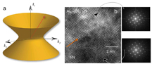 |
| "Hyperbolic metamaterials" could bring optical advances including powerful microscopes, quantum computers and high-performance solar cells. The graphic at left depicts a metamaterial's "hyperbolic dispersion" of light. At center is a high-resolution transmission electron microscope image showing the interface of titanium nitride and aluminum scandium nitride in a "superlattice" that is promising for potential applications. At right are two images created using a method called fast Fourier transform to see individual layers in the material. Purdue University image |
Abstract:
Epitaxial superlattices with titanium nitride as a plasmonic component for optical hyperbolic metamaterials
Gururaj V. Naik,1 Bivas Saha,2 Jing Liu,3 Sammy M. Saber,2 Eric Stach,2 Joseph MK Irudayaraj,3 Timothy D. Sands,1,2 Vladimir M. Shalaev1 and Alexandra Boltasseva*,1,4
1 School of Electrical and Computer Engineering, and Birck Nanotechnology Center, Purdue
University
2 School of Materials Engineering, and Birck Nanotechnology Center, Purdue University
3 Department of Agricultural and Biological Engineering, and Bindley Bioscience Center,
Purdue University
4 DTU Fotonik, Department of Photonics Engineering, Technical University of Denmark CORRESPONDING AUTHOR: *Alexandra Boltasseva
Titanium nitride (TiN) is a plasmonic material having optical properties resembling gold. Unlike gold however, TiN is CMOS-compatible, mechanically strong, and thermally stable at higher temperatures. Additionally, TiN can be grown in smooth, ultra-thin crystalline films, which are useful in constructing many plasmonic and metamaterial devices including hyperbolic metamaterials (HMMs). Hyperbolic metamaterials have been shown to exhibit exotic optical properties, including extremely high broadband photonic densities of states (PDOS), which are useful in quantum plasmonics applications. However, the extent to which the exotic properties of HMMs can be realized has been seriously limited by fabrication constraints and material properties. Here, we address these issues by realizing an epitaxial superlattice as an HMM. The superlattice consists of ultra-smooth layers as thin as 5 nm and exhibits sharp interfaces, which are essential for high-quality HMM devices. Our study reveals that such a TiN-based superlattice HMM provides a higher PDOS enhancement than gold- or silver-based HMMs. Given the advantages of TiN as a CMOS compatible plasmonic material, this demonstration brings a paradigm shift to the field of metamaterials similar to the way heterostructures did to the field of solid-state light sources.
Advance brings 'hyperbolic metamaterials' closer to reality
West Lafayette, IN | Posted on May 15th, 2014Researchers have taken a step toward practical applications for "hyperbolic metamaterials," ultra-thin crystalline films that could bring optical advances including powerful microscopes, quantum computers and high-performance solar cells.
New developments are reminiscent of advances that ushered in silicon chip technology, said Alexandra Boltasseva, a Purdue University associate professor of electrical and computer engineering.
Optical metamaterials harness clouds of electrons called surface plasmons to manipulate and control light. However, some of the plasmonic components under development rely on the use of metals such as gold and silver, which are incompatible with the complementary metal-oxide-semiconductor (CMOS) manufacturing process used to construct integrated circuits and do not transmit light efficiently.
Now researchers have shown how to create "superlattice" crystals from layers of the metal titanium nitride and aluminum scandium nitride, a dielectric, or insulator. Superlattices are crystals that can be grown continuously by adding new layers, a requirement for practical application.
"This work is a very important step in terms of fundamental contributions in materials science and optics as well as paving the way to some interesting applications," Boltasseva said. "We believe this demonstration brings a paradigm shift to the field of metamaterials similar to developments that led to dramatic advances in silicon technology."
Research findings are detailed in a paper appearing this week in the online Early Edition of Proceedings of the National Academy of Sciences.
Researchers created the superlattices using a method called epitaxy, "growing" the layers inside a vacuum chamber with a technique known as magnetron sputtering. It is difficult to use the technique to create structures that have sharply defined, ultra-thin and ultra-smooth layers of two different materials.
"This is one of the first reports of a metal-dielectric epitaxial superlattice," said Purdue doctoral student Bivas Saha, co-lead author of the PNAS paper with Gururaj V. Naik, a former Purdue doctoral student and now a postdoctoral scholar at Stanford University.
The list of possible applications for metamaterials includes a "planar hyperlens" that could make optical microscopes 10 times more powerful and able to see objects as small as DNA, advanced sensors, more efficient solar collectors, and quantum computing.
"Plasmonic and metamaterial devices require good material building blocks, both plasmonic and dielectric, in order to be useful in any real-world application," Boltasseva said. "Here, we develop both plasmonic and dielectric materials that can be grown epitaxially into ultra-thin and ultra-smooth layers with sharp interfaces."
Metamaterials have engineered surfaces that contain features, patterns or elements, such as tiny antennas or alternating layers of nitrides that enable unprecedented control of light. Under development for about 15 years, the metamaterials owe their unusual potential to precision design on the scale of nanometers.
The PNAS paper was authored by Naik; Saha; doctoral students Jing Liu and Sammy M. Saber; Eric Stach, a researcher at Brookhaven National Laboratory; Joseph Irudayaraj, a professor in Purdue's Department of Agricultural and Biological Engineering; Timothy D. Sands, executive vice president for academic affairs and provost and Basil S. Turner Professor of Engineering in the Schools of Materials Engineering and Electrical and Computer Engineering; Vladimir M. Shalaev, scientific director of nanophotonics at Purdue's Birck Nanotechnology Center and a distinguished professor of electrical and computer engineering; and Boltasseva.
"This work results from a unique collaboration between nanophotonics and materials science," Boltasseva said.
The hyperbolic metamaterial behaves as a metal when light is passing through it in one direction and like a dielectric in the perpendicular direction. This "extreme anisotropy" leads to "hyperbolic dispersion" of light and the ability to extract many more photons from devices than otherwise possible, resulting in high performance.
The layers of titanium nitride and aluminum scandium nitride used in this study are each about 5 to 20 nanometers thick. However, researchers have demonstrated that such superlattices can also be developed where the layers could be as thin as 2 nanometers, a tiny dimension only about eight atoms thick.
"People have tried for more than 50 years to combine metals and semiconductors with atomic-scale precision to build superlattices," Saha said. "However, this is one of the first demonstrations of achieving that step. The fascinating optical properties we see here are a manifestation of extraordinary structural control that we have achieved."
The feat is possible by choosing a metal and dielectric with compatible crystal structures, enabling the layers to grow together as a superlattice. The researchers alloyed aluminum nitride with scandium nitride, meaning the aluminum nitride is impregnated with scandium atoms to alter the material's crystal lattice to match titanium nitride's.
"The possibility of growing both metal and dielectric material components as a whole epitaxial system is indispensable for realizing high-performance metamaterials," Saha said. "One of the stumbling blocks is the fact that common dielectrics such as silica, alumina and other oxides cannot be used in combination with metallic components such as metal nitrides because the deposition processes are not compatible with each other."
Both of the materials should possess the same or compatible crystal structures.
"In general, a lattice mismatch of less than 5 percent is necessary for growing epitaxial quality films," he said.
A U.S. patent application has been filed through the Purdue Office of Technology Commercialization.
The material has been shown to work in a broad spectrum from near-infrared to visible light, potentially promising a wide array of applications.
"That's a novel part of this work - that we can create a superlattice metamaterial showing hyperbolic dispersion in the visible spectrum range," Boltasseva said.
The near-infrared is essential for telecommunications and optical communications, and visible light is important for sensors, microscopes and efficient solid-state light sources.
"Most interesting is the realm of quantum information technology," she said.
Computers based on quantum physics would have quantum bits, or "qubits," that exist in both the on and off states simultaneously, dramatically increasing the computer's power and memory. Quantum computers would take advantage of a phenomenon described by quantum theory called "entanglement." Instead of only the states of one and zero used in conventional computer processing, there are many possible "entangled quantum states" in between one and zero, increasing the capacity to process information.
The research has been funded in part by the U.S. Army Research Office and the National Science Foundation.
####
For more information, please click here
Contacts:
Writer:
Emil Venere
765-494-4709
Sources:
Alexandra Boltasseva
765-494-0301
Bivas Saha
Copyright © Purdue University
If you have a comment, please Contact us.Issuers of news releases, not 7th Wave, Inc. or Nanotechnology Now, are solely responsible for the accuracy of the content.
Bookmark:


| Related News Press |
News and information
![]() Quantum computer improves AI predictions April 17th, 2026
Quantum computer improves AI predictions April 17th, 2026
![]() Flexible sensor gains sensitivity under pressure April 17th, 2026
Flexible sensor gains sensitivity under pressure April 17th, 2026
![]() A reusable chip for particulate matter sensing April 17th, 2026
A reusable chip for particulate matter sensing April 17th, 2026
![]() Detecting vibrational quantum beating in the predissociation dynamics of SF6 using time-resolved photoelectron spectroscopy April 17th, 2026
Detecting vibrational quantum beating in the predissociation dynamics of SF6 using time-resolved photoelectron spectroscopy April 17th, 2026
Imaging
![]() Simple algorithm paired with standard imaging tool could predict failure in lithium metal batteries August 8th, 2025
Simple algorithm paired with standard imaging tool could predict failure in lithium metal batteries August 8th, 2025
![]() First real-time observation of two-dimensional melting process: Researchers at Mainz University unveil new insights into magnetic vortex structures August 8th, 2025
First real-time observation of two-dimensional melting process: Researchers at Mainz University unveil new insights into magnetic vortex structures August 8th, 2025
Thin films
![]() Tiny nanosheets, big leap: A new sensor detects ethanol at ultra-low levels January 30th, 2026
Tiny nanosheets, big leap: A new sensor detects ethanol at ultra-low levels January 30th, 2026
Govt.-Legislation/Regulation/Funding/Policy
![]() Quantum computer improves AI predictions April 17th, 2026
Quantum computer improves AI predictions April 17th, 2026
![]() Metasurfaces smooth light to boost magnetic sensing precision January 30th, 2026
Metasurfaces smooth light to boost magnetic sensing precision January 30th, 2026
![]() New imaging approach transforms study of bacterial biofilms August 8th, 2025
New imaging approach transforms study of bacterial biofilms August 8th, 2025
Quantum Computing
![]() Quantum computer improves AI predictions April 17th, 2026
Quantum computer improves AI predictions April 17th, 2026
![]() UC Irvine physicists discover method to reverse �quantum scrambling� : The work addresses the problem of information loss in quantum computing system April 17th, 2026
UC Irvine physicists discover method to reverse �quantum scrambling� : The work addresses the problem of information loss in quantum computing system April 17th, 2026
![]() Researchers develop molecular qubits that communicate at telecom frequencies October 3rd, 2025
Researchers develop molecular qubits that communicate at telecom frequencies October 3rd, 2025
Discoveries
![]() Quantum computer improves AI predictions April 17th, 2026
Quantum computer improves AI predictions April 17th, 2026
![]() Flexible sensor gains sensitivity under pressure April 17th, 2026
Flexible sensor gains sensitivity under pressure April 17th, 2026
![]() A reusable chip for particulate matter sensing April 17th, 2026
A reusable chip for particulate matter sensing April 17th, 2026
![]() Detecting vibrational quantum beating in the predissociation dynamics of SF6 using time-resolved photoelectron spectroscopy April 17th, 2026
Detecting vibrational quantum beating in the predissociation dynamics of SF6 using time-resolved photoelectron spectroscopy April 17th, 2026
Materials/Metamaterials/Magnetoresistance
![]() First real-time observation of two-dimensional melting process: Researchers at Mainz University unveil new insights into magnetic vortex structures August 8th, 2025
First real-time observation of two-dimensional melting process: Researchers at Mainz University unveil new insights into magnetic vortex structures August 8th, 2025
![]() Researchers unveil a groundbreaking clay-based solution to capture carbon dioxide and combat climate change June 6th, 2025
Researchers unveil a groundbreaking clay-based solution to capture carbon dioxide and combat climate change June 6th, 2025
![]() A 1960s idea inspires NBI researchers to study hitherto inaccessible quantum states June 6th, 2025
A 1960s idea inspires NBI researchers to study hitherto inaccessible quantum states June 6th, 2025
![]() Institute for Nanoscience hosts annual proposal planning meeting May 16th, 2025
Institute for Nanoscience hosts annual proposal planning meeting May 16th, 2025
Announcements
![]() A fundamentally new therapeutic approach to cystic fibrosis: Nanobody repairs cellular defect April 17th, 2026
A fundamentally new therapeutic approach to cystic fibrosis: Nanobody repairs cellular defect April 17th, 2026
![]() UC Irvine physicists discover method to reverse �quantum scrambling� : The work addresses the problem of information loss in quantum computing system April 17th, 2026
UC Irvine physicists discover method to reverse �quantum scrambling� : The work addresses the problem of information loss in quantum computing system April 17th, 2026
Interviews/Book Reviews/Essays/Reports/Podcasts/Journals/White papers/Posters
![]() A fundamentally new therapeutic approach to cystic fibrosis: Nanobody repairs cellular defect April 17th, 2026
A fundamentally new therapeutic approach to cystic fibrosis: Nanobody repairs cellular defect April 17th, 2026
![]() UC Irvine physicists discover method to reverse �quantum scrambling� : The work addresses the problem of information loss in quantum computing system April 17th, 2026
UC Irvine physicists discover method to reverse �quantum scrambling� : The work addresses the problem of information loss in quantum computing system April 17th, 2026
Tools
![]() Metasurfaces smooth light to boost magnetic sensing precision January 30th, 2026
Metasurfaces smooth light to boost magnetic sensing precision January 30th, 2026
![]() From sensors to smart systems: the rise of AI-driven photonic noses January 30th, 2026
From sensors to smart systems: the rise of AI-driven photonic noses January 30th, 2026
![]() Japan launches fully domestically produced quantum computer: Expo visitors to experience quantum computing firsthand August 8th, 2025
Japan launches fully domestically produced quantum computer: Expo visitors to experience quantum computing firsthand August 8th, 2025
Patents/IP/Tech Transfer/Licensing
![]() Getting drugs across the blood-brain barrier using nanoparticles March 3rd, 2023
Getting drugs across the blood-brain barrier using nanoparticles March 3rd, 2023
![]() Metasurfaces control polarized light at will: New research unlocks the hidden potential of metasurfaces August 13th, 2021
Metasurfaces control polarized light at will: New research unlocks the hidden potential of metasurfaces August 13th, 2021
![]() Arrowhead Pharmaceuticals Announces Closing of Agreement with Takeda November 27th, 2020
Arrowhead Pharmaceuticals Announces Closing of Agreement with Takeda November 27th, 2020
Military
![]() Quantum engineers �squeeze� laser frequency combs to make more sensitive gas sensors January 17th, 2025
Quantum engineers �squeeze� laser frequency combs to make more sensitive gas sensors January 17th, 2025
![]() Chainmail-like material could be the future of armor: First 2D mechanically interlocked polymer exhibits exceptional flexibility and strength January 17th, 2025
Chainmail-like material could be the future of armor: First 2D mechanically interlocked polymer exhibits exceptional flexibility and strength January 17th, 2025
![]() Single atoms show their true color July 5th, 2024
Single atoms show their true color July 5th, 2024
![]() NRL charters Navy�s quantum inertial navigation path to reduce drift April 5th, 2024
NRL charters Navy�s quantum inertial navigation path to reduce drift April 5th, 2024
Energy
![]() Sensors innovations for smart lithium-based batteries: advancements, opportunities, and potential challenges August 8th, 2025
Sensors innovations for smart lithium-based batteries: advancements, opportunities, and potential challenges August 8th, 2025
![]() Simple algorithm paired with standard imaging tool could predict failure in lithium metal batteries August 8th, 2025
Simple algorithm paired with standard imaging tool could predict failure in lithium metal batteries August 8th, 2025
Photonics/Optics/Lasers
![]() Metasurfaces smooth light to boost magnetic sensing precision January 30th, 2026
Metasurfaces smooth light to boost magnetic sensing precision January 30th, 2026
![]() From sensors to smart systems: the rise of AI-driven photonic noses January 30th, 2026
From sensors to smart systems: the rise of AI-driven photonic noses January 30th, 2026
Solar/Photovoltaic
![]() Spinel-type sulfide semiconductors to operate the next-generation LEDs and solar cells For solar-cell absorbers and green-LED source October 3rd, 2025
Spinel-type sulfide semiconductors to operate the next-generation LEDs and solar cells For solar-cell absorbers and green-LED source October 3rd, 2025
![]() KAIST researchers introduce new and improved, next-generation perovskite solar cell November 8th, 2024
KAIST researchers introduce new and improved, next-generation perovskite solar cell November 8th, 2024
![]() Groundbreaking precision in single-molecule optoelectronics August 16th, 2024
Groundbreaking precision in single-molecule optoelectronics August 16th, 2024
![]() Development of zinc oxide nanopagoda array photoelectrode: photoelectrochemical water-splitting hydrogen production January 12th, 2024
Development of zinc oxide nanopagoda array photoelectrode: photoelectrochemical water-splitting hydrogen production January 12th, 2024
Quantum nanoscience
![]() Beyond silicon: Electronics at the scale of a single molecule January 30th, 2026
Beyond silicon: Electronics at the scale of a single molecule January 30th, 2026
![]() MXene nanomaterials enter a new dimension Multilayer nanomaterial: MXene flakes created at Drexel University show new promise as 1D scrolls January 30th, 2026
MXene nanomaterials enter a new dimension Multilayer nanomaterial: MXene flakes created at Drexel University show new promise as 1D scrolls January 30th, 2026
![]() ICFO researchers overcome long-standing bottleneck in single photon detection with twisted 2D materials August 8th, 2025
ICFO researchers overcome long-standing bottleneck in single photon detection with twisted 2D materials August 8th, 2025
|
|
||
|
|
||
| The latest news from around the world, FREE | ||
|
|
||
|
|
||
| Premium Products | ||
|
|
||
|
Only the news you want to read!
Learn More |
||
|
|
||
|
Full-service, expert consulting
Learn More |
||
|
|
||