Home > Press > Genetic approach helps design broadband metamaterial
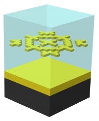 |
| Overall layers of the metamaterial absorber are shown. The black layer is the substrate, solid green layer is palladium, transparent blue layer is polyimide, broken green layer is the patterned layer and the transparent blue layer is again polyimide to seal and protect.
Credit: Bossard, Penn State |
Abstract:
A specially formed material that can provide custom broadband absorption in the infrared can be identified and manufactured using "genetic algorithms," according to Penn State engineers, who say these metamaterials can shield objects from view by infrared sensors, protect instruments and be manufactured to cover a variety of wavelengths. "The metamaterial has a high absorption over broad bandwidth," said Jeremy A. Bossard, postdoctoral fellow in electrical engineering.
Genetic approach helps design broadband metamaterial
University Park, PA | Posted on May 5th, 2014"Other screens have been developed for a narrow bandwidth, but this is the first that can cover a super-octave bandwidth in the infrared spectrum."
Having a broader bandwidth means that one material can protect against electromagnetic radiation over a wide range of wavelengths, making the material more useful. The researchers looked at silver, gold and palladium, but found that palladium provided better bandwidth coverage. This new metamaterial is actually made of layers on a silicon substrate or base. The first layer is palladium, followed by a polyimide layer. On top of this plastic layer is a palladium screen layer. The screen has elaborate, complicated cutouts -- sub wavelength geometry -- that serve to block the various wavelengths. A polyimide layer caps the whole absorber.
"As long as the properly designed pattern in the screen is much smaller than the wavelength, the material can work effectively as an absorber," said Lan Lin, graduate student in electrical engineering. "It can also absorb 90 percent of the infrared radiation that comes in at up to a 55 degree angle to the screen."
To design the necessary screen for this metamaterial, the researchers used a genetic algorithm. They described the screen pattern by a series of zeros and ones -- a chromosome -- and let the algorithm randomly select patterns to create an initial population of candidate designs. The algorithm then tested the patterns and eliminated all but the best. The best patterns were then randomly tweaked for the second generation. Again the algorithm discarded the worst and kept the best. After a number of generations the good patterns met and even exceeded the design goals. Along the way the best pattern from each generation was retained. They report their results in a recent issue of ACS Nano.
"We wouldn't be able to get an octave bandwidth coverage without the genetic algorithm," said Bossard. "In the past, researchers have tried to cover the bandwidth using multiple layers, but multiple layers were difficult to manufacture and register properly."
This evolved metamaterial can be easily manufactured because it is simply layers of metal or plastic that do not need complex alignment. The clear cap of polyimide serves to protect the screen, but also helps reduce any impedance mismatch that might occur when the wave moves from the air into the device.
"Genetic algorithms are used in electromagnetics, but we are at the forefront of using this method to design metamaterials," said Bossard.
###
Other researchers on this project included Seokho Yun, former postdoctoral fellow in electrical engineering, Liu Liu, graduate student in electrical engineering, Douglas H. Werner, McCain Chair Professor of Electrical Engineering, and Theresa Meyer, Distinguished Professor of Electrical Engineering and Materials Science and Engineering, all at Penn State.
The National Science Foundation supported this work.
####
For more information, please click here
Contacts:
A'ndrea Elyse Messer
814-865-9481
Copyright © Penn State
If you have a comment, please Contact us.Issuers of news releases, not 7th Wave, Inc. or Nanotechnology Now, are solely responsible for the accuracy of the content.
Bookmark:


| Related News Press |
News and information
![]() Quantum computer improves AI predictions April 17th, 2026
Quantum computer improves AI predictions April 17th, 2026
![]() Flexible sensor gains sensitivity under pressure April 17th, 2026
Flexible sensor gains sensitivity under pressure April 17th, 2026
![]() A reusable chip for particulate matter sensing April 17th, 2026
A reusable chip for particulate matter sensing April 17th, 2026
![]() Detecting vibrational quantum beating in the predissociation dynamics of SF6 using time-resolved photoelectron spectroscopy April 17th, 2026
Detecting vibrational quantum beating in the predissociation dynamics of SF6 using time-resolved photoelectron spectroscopy April 17th, 2026
Govt.-Legislation/Regulation/Funding/Policy
![]() Quantum computer improves AI predictions April 17th, 2026
Quantum computer improves AI predictions April 17th, 2026
![]() Metasurfaces smooth light to boost magnetic sensing precision January 30th, 2026
Metasurfaces smooth light to boost magnetic sensing precision January 30th, 2026
![]() New imaging approach transforms study of bacterial biofilms August 8th, 2025
New imaging approach transforms study of bacterial biofilms August 8th, 2025
Sensors
![]() Flexible sensor gains sensitivity under pressure April 17th, 2026
Flexible sensor gains sensitivity under pressure April 17th, 2026
![]() Tiny nanosheets, big leap: A new sensor detects ethanol at ultra-low levels January 30th, 2026
Tiny nanosheets, big leap: A new sensor detects ethanol at ultra-low levels January 30th, 2026
![]() From sensors to smart systems: the rise of AI-driven photonic noses January 30th, 2026
From sensors to smart systems: the rise of AI-driven photonic noses January 30th, 2026
![]() Sensors innovations for smart lithium-based batteries: advancements, opportunities, and potential challenges August 8th, 2025
Sensors innovations for smart lithium-based batteries: advancements, opportunities, and potential challenges August 8th, 2025
Discoveries
![]() Quantum computer improves AI predictions April 17th, 2026
Quantum computer improves AI predictions April 17th, 2026
![]() Flexible sensor gains sensitivity under pressure April 17th, 2026
Flexible sensor gains sensitivity under pressure April 17th, 2026
![]() A reusable chip for particulate matter sensing April 17th, 2026
A reusable chip for particulate matter sensing April 17th, 2026
![]() Detecting vibrational quantum beating in the predissociation dynamics of SF6 using time-resolved photoelectron spectroscopy April 17th, 2026
Detecting vibrational quantum beating in the predissociation dynamics of SF6 using time-resolved photoelectron spectroscopy April 17th, 2026
Materials/Metamaterials/Magnetoresistance
![]() First real-time observation of two-dimensional melting process: Researchers at Mainz University unveil new insights into magnetic vortex structures August 8th, 2025
First real-time observation of two-dimensional melting process: Researchers at Mainz University unveil new insights into magnetic vortex structures August 8th, 2025
![]() Researchers unveil a groundbreaking clay-based solution to capture carbon dioxide and combat climate change June 6th, 2025
Researchers unveil a groundbreaking clay-based solution to capture carbon dioxide and combat climate change June 6th, 2025
![]() A 1960s idea inspires NBI researchers to study hitherto inaccessible quantum states June 6th, 2025
A 1960s idea inspires NBI researchers to study hitherto inaccessible quantum states June 6th, 2025
![]() Institute for Nanoscience hosts annual proposal planning meeting May 16th, 2025
Institute for Nanoscience hosts annual proposal planning meeting May 16th, 2025
Announcements
![]() A fundamentally new therapeutic approach to cystic fibrosis: Nanobody repairs cellular defect April 17th, 2026
A fundamentally new therapeutic approach to cystic fibrosis: Nanobody repairs cellular defect April 17th, 2026
![]() UC Irvine physicists discover method to reverse �quantum scrambling� : The work addresses the problem of information loss in quantum computing system April 17th, 2026
UC Irvine physicists discover method to reverse �quantum scrambling� : The work addresses the problem of information loss in quantum computing system April 17th, 2026
Interviews/Book Reviews/Essays/Reports/Podcasts/Journals/White papers/Posters
![]() A fundamentally new therapeutic approach to cystic fibrosis: Nanobody repairs cellular defect April 17th, 2026
A fundamentally new therapeutic approach to cystic fibrosis: Nanobody repairs cellular defect April 17th, 2026
![]() UC Irvine physicists discover method to reverse �quantum scrambling� : The work addresses the problem of information loss in quantum computing system April 17th, 2026
UC Irvine physicists discover method to reverse �quantum scrambling� : The work addresses the problem of information loss in quantum computing system April 17th, 2026
Military
![]() Quantum engineers �squeeze� laser frequency combs to make more sensitive gas sensors January 17th, 2025
Quantum engineers �squeeze� laser frequency combs to make more sensitive gas sensors January 17th, 2025
![]() Chainmail-like material could be the future of armor: First 2D mechanically interlocked polymer exhibits exceptional flexibility and strength January 17th, 2025
Chainmail-like material could be the future of armor: First 2D mechanically interlocked polymer exhibits exceptional flexibility and strength January 17th, 2025
![]() Single atoms show their true color July 5th, 2024
Single atoms show their true color July 5th, 2024
![]() NRL charters Navy�s quantum inertial navigation path to reduce drift April 5th, 2024
NRL charters Navy�s quantum inertial navigation path to reduce drift April 5th, 2024
|
|
||
|
|
||
| The latest news from around the world, FREE | ||
|
|
||
|
|
||
| Premium Products | ||
|
|
||
|
Only the news you want to read!
Learn More |
||
|
|
||
|
Full-service, expert consulting
Learn More |
||
|
|
||