Home > Press > UNIST research team opens graphene band-gap
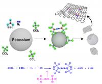 |
| This is a schematic representation for the formation of BCN-graphene via solvothermal reaction between carbon tetrachloride (CCl4) boron tribromide (BBr3) and nitrogen (N2) in the presence of potassium (K).
Credit: UNIST |
Abstract:
Ulsan National Institute of Science and Technology (UNIST) announced a method for the mass production of boron/nitrogen co-doped graphene nanoplatelets, which led to the fabrication of a graphene-based field -effect transistor (FET) with semiconducting nature. This opens up opportunities for practical use in electronic devices.
UNIST research team opens graphene band-gap
Ulsan, Korea | Posted on December 18th, 2013The Ulsan National Institute of Science and Technology (UNIST) research team led by Prof. Jong-Beom Baek have discovered an efficient method for the mass production of boron/nitrogen co-doped graphene nanoplatelets (BCN-graphene) via a simple solvothermal reaction of BBr3/CCl4/N2 in the presence of potassium. This work was published in "Angewandte Chemie International Edition" as a VIP ("Very Important Paper".
Since graphene was experimentally discovered in 2004, it has been the focus of vigorous applied research due to its outstanding properties such as high specific surface area, good thermal and electrical conductivities, and many more properties.
However, its Achilles heel is a vanishing band-gap for semiconductor application. As a result, it is not suitable for logic applications, because devices cannot be switched off. Therefore, graphene must be modified to produce a band-gap, if it is to be used in electronic devices.
Various methods of making graphene-based field effect transistors (FETs) have been exploited, including doping graphene, tailoring graphene-like a nanoribbon, and using boron nitride as a support. Among the methods of controlling the band-gap of graphene, doping methods show the most promisinge in terms of industrial scale feasibility.
Although world leading researchers have tried to add boron into graphitic framework to open its band-gap for semiconductor applications, there has not been any notable success yet. Since the atomic size of boron (85 pm) is larger than that of carbon (77 pm), it is difficult to accommodate boron into the graphitic network structure.
A new synthetic protocol developed by a research team from UNIST, a leading Korean university, has revealed that boron/nitrogen co-doping is only feasible when carbon tetrachloride (CCl4 ) is treated with boron tribromide (BBr3 ) and nitrogen (N2) gas.
In order to help boron-doping into graphene structure, the research team used nitrogen (70 pm), which is a bit smaller than carbon and boron. The idea was very simple, but the result was surprising. Pairing two nitrogen atoms and two boron atoms can compensate for the atomic size mismatch. Thus, boron and nitrogen pairs can be easily introduced into the graphitic network. The resultant BCN-graphene generates a band-gap for FETs.
"Although the performance of the FET is not in the ranges of commercial silicon-based semiconductors, this initiative work should be the proof of a new concept and a great leap forward for studying graphene with band-gap opening," said Prof. Jong-Beom Baek.
"I believe this work is one of the biggest advancements in considering the viability of a simple synthetic approach," said Ph.D. candidate Sun-Min Jung, the first author of this article.
Prof. Baek explains the next step: "Now, the remaining challenge is fine-tuning a band-gap to improve the on/off current ratio for real device applications."
###
Information about the research
Other researchers in the team include Profs. Joon Hak Oh, Noejung Park, HuYoung Jeong and 6 graduate students.
The research work was funded by the National Research Foundation (NRF) of Korea, and the US Air Force Office of Scientific Research through the Asian Office of Aerospace R&D (AFOSR-AOARD).
####
For more information, please click here
Contacts:
Hyunho Lee
Copyright © Ulsan National Institute of Science and Technology(UNIST)
If you have a comment, please Contact us.Issuers of news releases, not 7th Wave, Inc. or Nanotechnology Now, are solely responsible for the accuracy of the content.
Bookmark:


| Related Links |
![]() Ulsan National Institute of Science and Technology:
Ulsan National Institute of Science and Technology:
| Related News Press |
News and information
![]() Quantum computer improves AI predictions April 17th, 2026
Quantum computer improves AI predictions April 17th, 2026
![]() Flexible sensor gains sensitivity under pressure April 17th, 2026
Flexible sensor gains sensitivity under pressure April 17th, 2026
![]() A reusable chip for particulate matter sensing April 17th, 2026
A reusable chip for particulate matter sensing April 17th, 2026
![]() Detecting vibrational quantum beating in the predissociation dynamics of SF6 using time-resolved photoelectron spectroscopy April 17th, 2026
Detecting vibrational quantum beating in the predissociation dynamics of SF6 using time-resolved photoelectron spectroscopy April 17th, 2026
Graphene/ Graphite
![]() Electrifying results shed light on graphene foam as a potential material for lab grown cartilage June 6th, 2025
Electrifying results shed light on graphene foam as a potential material for lab grown cartilage June 6th, 2025
![]() Breakthrough in proton barrier films using pore-free graphene oxide: Kumamoto University researchers achieve new milestone in advanced coating technologies September 13th, 2024
Breakthrough in proton barrier films using pore-free graphene oxide: Kumamoto University researchers achieve new milestone in advanced coating technologies September 13th, 2024
Govt.-Legislation/Regulation/Funding/Policy
![]() Quantum computer improves AI predictions April 17th, 2026
Quantum computer improves AI predictions April 17th, 2026
![]() Metasurfaces smooth light to boost magnetic sensing precision January 30th, 2026
Metasurfaces smooth light to boost magnetic sensing precision January 30th, 2026
![]() New imaging approach transforms study of bacterial biofilms August 8th, 2025
New imaging approach transforms study of bacterial biofilms August 8th, 2025
Chip Technology
![]() A reusable chip for particulate matter sensing April 17th, 2026
A reusable chip for particulate matter sensing April 17th, 2026
![]() Metasurfaces smooth light to boost magnetic sensing precision January 30th, 2026
Metasurfaces smooth light to boost magnetic sensing precision January 30th, 2026
Discoveries
![]() Quantum computer improves AI predictions April 17th, 2026
Quantum computer improves AI predictions April 17th, 2026
![]() Flexible sensor gains sensitivity under pressure April 17th, 2026
Flexible sensor gains sensitivity under pressure April 17th, 2026
![]() A reusable chip for particulate matter sensing April 17th, 2026
A reusable chip for particulate matter sensing April 17th, 2026
![]() Detecting vibrational quantum beating in the predissociation dynamics of SF6 using time-resolved photoelectron spectroscopy April 17th, 2026
Detecting vibrational quantum beating in the predissociation dynamics of SF6 using time-resolved photoelectron spectroscopy April 17th, 2026
Announcements
![]() A fundamentally new therapeutic approach to cystic fibrosis: Nanobody repairs cellular defect April 17th, 2026
A fundamentally new therapeutic approach to cystic fibrosis: Nanobody repairs cellular defect April 17th, 2026
![]() UC Irvine physicists discover method to reverse �quantum scrambling� : The work addresses the problem of information loss in quantum computing system April 17th, 2026
UC Irvine physicists discover method to reverse �quantum scrambling� : The work addresses the problem of information loss in quantum computing system April 17th, 2026
Interviews/Book Reviews/Essays/Reports/Podcasts/Journals/White papers/Posters
![]() A fundamentally new therapeutic approach to cystic fibrosis: Nanobody repairs cellular defect April 17th, 2026
A fundamentally new therapeutic approach to cystic fibrosis: Nanobody repairs cellular defect April 17th, 2026
![]() UC Irvine physicists discover method to reverse �quantum scrambling� : The work addresses the problem of information loss in quantum computing system April 17th, 2026
UC Irvine physicists discover method to reverse �quantum scrambling� : The work addresses the problem of information loss in quantum computing system April 17th, 2026
Military
![]() Quantum engineers �squeeze� laser frequency combs to make more sensitive gas sensors January 17th, 2025
Quantum engineers �squeeze� laser frequency combs to make more sensitive gas sensors January 17th, 2025
![]() Chainmail-like material could be the future of armor: First 2D mechanically interlocked polymer exhibits exceptional flexibility and strength January 17th, 2025
Chainmail-like material could be the future of armor: First 2D mechanically interlocked polymer exhibits exceptional flexibility and strength January 17th, 2025
![]() Single atoms show their true color July 5th, 2024
Single atoms show their true color July 5th, 2024
![]() NRL charters Navy�s quantum inertial navigation path to reduce drift April 5th, 2024
NRL charters Navy�s quantum inertial navigation path to reduce drift April 5th, 2024
|
|
||
|
|
||
| The latest news from around the world, FREE | ||
|
|
||
|
|
||
| Premium Products | ||
|
|
||
|
Only the news you want to read!
Learn More |
||
|
|
||
|
Full-service, expert consulting
Learn More |
||
|
|
||