Home > Press > Nanotubes can solder themselves, markedly improving device performance
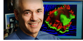 |
| Electrical and computer engineering professor Joseph Lyding led the research team that developed a way to heal gaps in wires too small for even the world's tiniest soldering iron. Photo by L. Brian Stauffer |
Abstract:
University of Illinois researchers have developed a way to heal gaps in wires too small for even the world's tiniest soldering iron.
Nanotubes can solder themselves, markedly improving device performance
Champaign, IL | Posted on November 25th, 2013Led by electrical and computer engineering professor Joseph Lyding and graduate student Jae Won Do, the Illinois team published its results in the journal Nano Letters.
Carbon nanotubes are like tiny hollow wires of carbon just 1 atom thick - similar to graphene but cylindrical. Researchers have been exploring using them as transistors instead of traditional silicon, because carbon nanotubes are easier to transport onto alternate substrates, such as thin sheets of plastic, for low-cost flexible electronics or flat-panel displays. (See video for demonstration of the process.)
Carbon nanotubes themselves are high-quality conductors, but creating single tubes suitable to serve as transistors is very difficult. Arrays of nanotubes are much easier to make, but the current has to hop through junctions from one nanotube to the next, slowing it down. In standard electrical wires, such junctions would be soldered, but how could the gaps be bridged on such a small scale?
"It occurred to me that these nanotube junctions will get hot when you pass current through them," said Lyding, "kind of like faulty wiring in a home can create hot spots. In our case, we use these hot spots to trigger a local chemical reaction that deposits metal that nano-solders the junctions."
Lyding's group teamed with Eric Pop, an adjunct professor of electrical and computer engineering, and John Rogers, Swanlund professor in materials science and engineering, experts on carbon nanotube synthesis and transfer, as well as chemistry professor Greg Girolami. Girolami is an expert in a process that uses gases to deposit metals on a surface, called chemical vapor deposition (CVD).
The nano-soldering process is simple and self-regulating. A carbon nanotube array is placed in a chamber pumped full of the metal-containing gas molecules. When a current passes through the transistor, the junctions heat because of resistance as electrons flow from one nanotube to the next. The molecules react to the heat, depositing the metal at the hot spots and effectively "soldering" the junctions. Then the resistance drops, as well as the temperature, so the reaction stops.
The nano-soldering takes only seconds and improves the device performance by an order of magnitude - almost to the level of devices made from single nanotubes, but much easier to manufacture on a large scale.
"It would be easy to insert the CVD process in existing process flows," Lyding said. "CVD technology is commercially available off-the-shelf. People can fabricate these transistors with the ability to turn them on so that this process can be done. Then when it's finished they can finish the wiring and connect them into the circuits. Ultimately it would be a low-cost procedure."
Now, the group is working to refine the process.
"We think we can make it even better," Lyding said. "This is the prelude, we hope, but it's actually quite significant."
The National Science Foundation and the Office of Naval Research supported this work. Lyding and Rogers also are affiliated with the Beckman Institute for Advanced Science and Technology at the U. of I.
####
For more information, please click here
Contacts:
Liz Ahlberg
Physical Sciences Editor
217-244-1073
Joe Lyding
217-333-8370
Copyright © University of Illinois at Urbana-Champaign
If you have a comment, please Contact us.Issuers of news releases, not 7th Wave, Inc. or Nanotechnology Now, are solely responsible for the accuracy of the content.
Bookmark:


| Related Links |
| Related News Press |
News and information
![]() Quantum computer improves AI predictions April 17th, 2026
Quantum computer improves AI predictions April 17th, 2026
![]() Flexible sensor gains sensitivity under pressure April 17th, 2026
Flexible sensor gains sensitivity under pressure April 17th, 2026
![]() A reusable chip for particulate matter sensing April 17th, 2026
A reusable chip for particulate matter sensing April 17th, 2026
![]() Detecting vibrational quantum beating in the predissociation dynamics of SF6 using time-resolved photoelectron spectroscopy April 17th, 2026
Detecting vibrational quantum beating in the predissociation dynamics of SF6 using time-resolved photoelectron spectroscopy April 17th, 2026
Display technology/LEDs/SS Lighting/OLEDs
![]() Spinel-type sulfide semiconductors to operate the next-generation LEDs and solar cells For solar-cell absorbers and green-LED source October 3rd, 2025
Spinel-type sulfide semiconductors to operate the next-generation LEDs and solar cells For solar-cell absorbers and green-LED source October 3rd, 2025
Videos/Movies
![]() ICFO researchers overcome long-standing bottleneck in single photon detection with twisted 2D materials August 8th, 2025
ICFO researchers overcome long-standing bottleneck in single photon detection with twisted 2D materials August 8th, 2025
Graphene/ Graphite
![]() Electrifying results shed light on graphene foam as a potential material for lab grown cartilage June 6th, 2025
Electrifying results shed light on graphene foam as a potential material for lab grown cartilage June 6th, 2025
![]() Breakthrough in proton barrier films using pore-free graphene oxide: Kumamoto University researchers achieve new milestone in advanced coating technologies September 13th, 2024
Breakthrough in proton barrier films using pore-free graphene oxide: Kumamoto University researchers achieve new milestone in advanced coating technologies September 13th, 2024
Chip Technology
![]() A reusable chip for particulate matter sensing April 17th, 2026
A reusable chip for particulate matter sensing April 17th, 2026
![]() Metasurfaces smooth light to boost magnetic sensing precision January 30th, 2026
Metasurfaces smooth light to boost magnetic sensing precision January 30th, 2026
Nanotubes/Buckyballs/Fullerenes/Nanorods/Nanostrings/Nanosheets
![]() Tiny nanosheets, big leap: A new sensor detects ethanol at ultra-low levels January 30th, 2026
Tiny nanosheets, big leap: A new sensor detects ethanol at ultra-low levels January 30th, 2026
![]() Enhancing power factor of p- and n-type single-walled carbon nanotubes April 25th, 2025
Enhancing power factor of p- and n-type single-walled carbon nanotubes April 25th, 2025
![]() Chainmail-like material could be the future of armor: First 2D mechanically interlocked polymer exhibits exceptional flexibility and strength January 17th, 2025
Chainmail-like material could be the future of armor: First 2D mechanically interlocked polymer exhibits exceptional flexibility and strength January 17th, 2025
![]() Innovative biomimetic superhydrophobic coating combines repair and buffering properties for superior anti-erosion December 13th, 2024
Innovative biomimetic superhydrophobic coating combines repair and buffering properties for superior anti-erosion December 13th, 2024
Discoveries
![]() Quantum computer improves AI predictions April 17th, 2026
Quantum computer improves AI predictions April 17th, 2026
![]() Flexible sensor gains sensitivity under pressure April 17th, 2026
Flexible sensor gains sensitivity under pressure April 17th, 2026
![]() A reusable chip for particulate matter sensing April 17th, 2026
A reusable chip for particulate matter sensing April 17th, 2026
![]() Detecting vibrational quantum beating in the predissociation dynamics of SF6 using time-resolved photoelectron spectroscopy April 17th, 2026
Detecting vibrational quantum beating in the predissociation dynamics of SF6 using time-resolved photoelectron spectroscopy April 17th, 2026
Announcements
![]() A fundamentally new therapeutic approach to cystic fibrosis: Nanobody repairs cellular defect April 17th, 2026
A fundamentally new therapeutic approach to cystic fibrosis: Nanobody repairs cellular defect April 17th, 2026
![]() UC Irvine physicists discover method to reverse �quantum scrambling� : The work addresses the problem of information loss in quantum computing system April 17th, 2026
UC Irvine physicists discover method to reverse �quantum scrambling� : The work addresses the problem of information loss in quantum computing system April 17th, 2026
Interviews/Book Reviews/Essays/Reports/Podcasts/Journals/White papers/Posters
![]() A fundamentally new therapeutic approach to cystic fibrosis: Nanobody repairs cellular defect April 17th, 2026
A fundamentally new therapeutic approach to cystic fibrosis: Nanobody repairs cellular defect April 17th, 2026
![]() UC Irvine physicists discover method to reverse �quantum scrambling� : The work addresses the problem of information loss in quantum computing system April 17th, 2026
UC Irvine physicists discover method to reverse �quantum scrambling� : The work addresses the problem of information loss in quantum computing system April 17th, 2026
|
|
||
|
|
||
| The latest news from around the world, FREE | ||
|
|
||
|
|
||
| Premium Products | ||
|
|
||
|
Only the news you want to read!
Learn More |
||
|
|
||
|
Full-service, expert consulting
Learn More |
||
|
|
||