Home > Press > ASU, Georgia Tech create breakthrough for solar cell efficiency: New atomic layer-by-layer InGaN technology offers perfect crystal
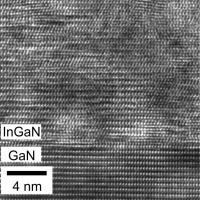 |
| The atomic arrangement at a relaxed InGaN/GaN interface created by layer-by-layer atomic crystal growth is shown. The technique may point to new developments in solar cell efficiency.
Credit: Arizona State University |
Abstract:
Did you know that crystals form the basis for the penetrating icy blue glare of car headlights and could be fundamental to the future in solar energy technology?
Crystals are at the heart of diodes. Not the kind you might find in quartz, formed naturally, but manufactured to form alloys, such as indium gallium nitride or InGaN. This alloy forms the light emitting region of LEDs, for illumination in the visible range, and of laser diodes (LDs) in the blue-UV range.
ASU, Georgia Tech create breakthrough for solar cell efficiency: New atomic layer-by-layer InGaN technology offers perfect crystal
Tempe, AZ and Atlanta, GA | Posted on October 26th, 2013Research into making better crystals, with high crystalline quality, light emission efficiency and luminosity, is also at the heart of studies being done at Arizona State University by Research Scientist Alec Fischer and Doctoral Candidate Yong Wei in Professor Fernando Ponce's group in the Department of Physics.
In an article recently published in the journal Applied Physics Letters, the ASU group, in collaboration with a scientific team led by Professor Alan Doolittle at the Georgia Institute of Technology, has just revealed the fundamental aspect of a new approach to growing InGaN crystals for diodes, which promises to move photovoltaic solar cell technology toward record-breaking efficiencies.
The InGaN crystals are grown as layers in a sandwich-like arrangement on sapphire substrates. Typically, researchers have found that the atomic separation of the layers varies; a condition that can lead to high levels of strain, breakdowns in growth, and fluctuations in the alloy's chemical composition.
"Being able to ease the strain and increase the uniformity in the composition of InGaN is very desirable," says Ponce, "but difficult to achieve. Growth of these layers is similar to trying to smoothly fit together two honeycombs with different cell sizes, where size difference disrupts a periodic arrangement of the cells."
As outlined in their publication, the authors developed an approach where pulses of molecules were introduced to achieve the desired alloy composition. The method, developed by Doolittle, is called metal-modulated epitaxy. "This technique allows an atomic layer-by-layer growth of the material," says Ponce.
Analysis of the atomic arrangement and the luminosity at the nanoscale level was performed by Fischer, the lead author of the study, and Wei. Their results showed that the films grown with the epitaxy technique had almost ideal characteristics and revealed that the unexpected results came from the strain relaxation at the first atomic layer of crystal growth.
"Doolittle's group was able to assemble a final crystal that is more uniform and whose lattice structures match up�resulting in a film that resembles a perfect crystal," says Ponce. "The luminosity was also like that of a perfect crystal. Something that no one in our field thought was possible."
The ASU and Georgia Tech team's elimination of these two seemingly insurmountable defects (non-uniform composition and mismatched lattice alignment) ultimately means that LEDs and solar photovoltaic products can now be developed that have much higher, efficient performance.
"While we are still a ways off from record-setting solar cells, this breakthrough could have immediate and lasting impact on light emitting devices and could potentially make the second most abundant semiconductor family, III-Nitrides, a real player in the solar cell field," says Doolittle. Doolittle's team at Georgia Tech's School of Electrical and Computer Engineering also included Michael Moseley and Brendan Gunning. A patent is pending for the new technology.
####
For more information, please click here
Contacts:
Margaret Coulombe
480-727-8934
Copyright © Arizona State University
If you have a comment, please Contact us.Issuers of news releases, not 7th Wave, Inc. or Nanotechnology Now, are solely responsible for the accuracy of the content.
Bookmark:


| Related News Press |
News and information
![]() Quantum computer improves AI predictions April 17th, 2026
Quantum computer improves AI predictions April 17th, 2026
![]() Flexible sensor gains sensitivity under pressure April 17th, 2026
Flexible sensor gains sensitivity under pressure April 17th, 2026
![]() A reusable chip for particulate matter sensing April 17th, 2026
A reusable chip for particulate matter sensing April 17th, 2026
![]() Detecting vibrational quantum beating in the predissociation dynamics of SF6 using time-resolved photoelectron spectroscopy April 17th, 2026
Detecting vibrational quantum beating in the predissociation dynamics of SF6 using time-resolved photoelectron spectroscopy April 17th, 2026
Display technology/LEDs/SS Lighting/OLEDs
![]() Spinel-type sulfide semiconductors to operate the next-generation LEDs and solar cells For solar-cell absorbers and green-LED source October 3rd, 2025
Spinel-type sulfide semiconductors to operate the next-generation LEDs and solar cells For solar-cell absorbers and green-LED source October 3rd, 2025
![]() Efficient and stable hybrid perovskite-organic light-emitting diodes with external quantum efficiency exceeding 40 per cent July 5th, 2024
Efficient and stable hybrid perovskite-organic light-emitting diodes with external quantum efficiency exceeding 40 per cent July 5th, 2024
Discoveries
![]() Quantum computer improves AI predictions April 17th, 2026
Quantum computer improves AI predictions April 17th, 2026
![]() Flexible sensor gains sensitivity under pressure April 17th, 2026
Flexible sensor gains sensitivity under pressure April 17th, 2026
![]() A reusable chip for particulate matter sensing April 17th, 2026
A reusable chip for particulate matter sensing April 17th, 2026
![]() Detecting vibrational quantum beating in the predissociation dynamics of SF6 using time-resolved photoelectron spectroscopy April 17th, 2026
Detecting vibrational quantum beating in the predissociation dynamics of SF6 using time-resolved photoelectron spectroscopy April 17th, 2026
Announcements
![]() A fundamentally new therapeutic approach to cystic fibrosis: Nanobody repairs cellular defect April 17th, 2026
A fundamentally new therapeutic approach to cystic fibrosis: Nanobody repairs cellular defect April 17th, 2026
![]() UC Irvine physicists discover method to reverse �quantum scrambling� : The work addresses the problem of information loss in quantum computing system April 17th, 2026
UC Irvine physicists discover method to reverse �quantum scrambling� : The work addresses the problem of information loss in quantum computing system April 17th, 2026
Patents/IP/Tech Transfer/Licensing
![]() Getting drugs across the blood-brain barrier using nanoparticles March 3rd, 2023
Getting drugs across the blood-brain barrier using nanoparticles March 3rd, 2023
![]() Metasurfaces control polarized light at will: New research unlocks the hidden potential of metasurfaces August 13th, 2021
Metasurfaces control polarized light at will: New research unlocks the hidden potential of metasurfaces August 13th, 2021
![]() Arrowhead Pharmaceuticals Announces Closing of Agreement with Takeda November 27th, 2020
Arrowhead Pharmaceuticals Announces Closing of Agreement with Takeda November 27th, 2020
Energy
![]() Sensors innovations for smart lithium-based batteries: advancements, opportunities, and potential challenges August 8th, 2025
Sensors innovations for smart lithium-based batteries: advancements, opportunities, and potential challenges August 8th, 2025
![]() Simple algorithm paired with standard imaging tool could predict failure in lithium metal batteries August 8th, 2025
Simple algorithm paired with standard imaging tool could predict failure in lithium metal batteries August 8th, 2025
Research partnerships
![]() Lab to industry: InSe wafer-scale breakthrough for future electronics August 8th, 2025
Lab to industry: InSe wafer-scale breakthrough for future electronics August 8th, 2025
![]() HKU physicists uncover hidden order in the quantum world through deconfined quantum critical points April 25th, 2025
HKU physicists uncover hidden order in the quantum world through deconfined quantum critical points April 25th, 2025
Solar/Photovoltaic
![]() Spinel-type sulfide semiconductors to operate the next-generation LEDs and solar cells For solar-cell absorbers and green-LED source October 3rd, 2025
Spinel-type sulfide semiconductors to operate the next-generation LEDs and solar cells For solar-cell absorbers and green-LED source October 3rd, 2025
![]() KAIST researchers introduce new and improved, next-generation perovskite solar cell November 8th, 2024
KAIST researchers introduce new and improved, next-generation perovskite solar cell November 8th, 2024
![]() Groundbreaking precision in single-molecule optoelectronics August 16th, 2024
Groundbreaking precision in single-molecule optoelectronics August 16th, 2024
![]() Development of zinc oxide nanopagoda array photoelectrode: photoelectrochemical water-splitting hydrogen production January 12th, 2024
Development of zinc oxide nanopagoda array photoelectrode: photoelectrochemical water-splitting hydrogen production January 12th, 2024
|
|
||
|
|
||
| The latest news from around the world, FREE | ||
|
|
||
|
|
||
| Premium Products | ||
|
|
||
|
Only the news you want to read!
Learn More |
||
|
|
||
|
Full-service, expert consulting
Learn More |
||
|
|
||