Home > Press > Promising new alloy for resistive switching memory: Tiny nanoscale filaments could be breakthrough for smaller, denser memory devices
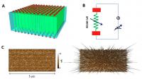 |
| (A) This is an illustration of the RRAM array with each memory cell comprising of one filament (sandwiched between two electrodes). In comparison to the surrounding insulator matrix, a number of nano-filaments are formed within the bulk oxide. (B) This is a basic element of a RRAM cell. Control of the electrical field leads to different resistance states. (C) Localized formation of conductive filaments in a TiO2 thin film is shown. The left shows the conductivity map recorded by CAFM. The right shows the same current mapping in 3D.
Credit: Yuanmin Du/National U.Singapore |
Abstract:
Memory based on electrically-induced "resistive switching" effects have generated a great deal of interest among engineers searching for faster and smaller devices because resistive switching would allow for a higher memory density.
Promising new alloy for resistive switching memory: Tiny nanoscale filaments could be breakthrough for smaller, denser memory devices
Washington, DC | Posted on September 21st, 2013Researchers have tested a number of oxide materials for their promise in resistive switching memories, and now a team of researchers in Singapore have demonstrated how conductive nano-filaments in amorphous titanium dioxide (TiO2) thin films could be utilized for resistive switching device applications.
Yuanmin Du, Andrew Thye Shen Wee and researchers from the National University of Singapore and the Agency for Science, Technology and Research (A*STAR) of Singapore, describe their results in the journal AIP Advances, which is produced by AIP Publishing.
How Resistive Switching Works
The basic idea of a resistive switching device is that an oxide, which normally acts as an insulator, can be transformed into a conductor, creating a nanoscale filament by using a sufficiently high voltage. With a RRAM (Resistive Random-Access Memory) device comprising of a single filament, two distinct resistance states ("1" and "0") can be obtained through a simple process of filament rupture and re-formation.
The conductivity of the oxide thin films can be adjusted by changing the deposition conditions. "During the measurements of the as-deposited amorphous TiO2 based resistive switching devices, it was found that the oxide thin films initially have good conductivity. This implies that a high electrical breakdown initialization process is not required, as reported in many other switching devices using highly insulating oxide thin films," says Du. "The Conductive Atomic Force Microscopy (CAFM) experiments further confirmed that it is possible to form conductive filaments in oxide thin films through a localized transition by an electrical field."
This research team applied both CAFM and KPFM (Kelvin Probe Force Microscopy), a unique approach that allowed the explanation of the observed resistive switching phenomena. Instead of treating filamentary and interfacial effects separately as done previously, both effects were integrated into one filament-interface model, which could help guide the design of RRAM based devices.
The evidence of high density and uniformly distributed nano-filaments implies that high-density memory cells could be made using such oxide thin films. Such materials are promising for future applications. The small dimension of the formed filament provides great advantages over current technology, as Du explains. "In addition to TiO2, we believe that many other oxides could also have the similar properties."
####
About American Institute of Physics
AIP Advances is a fully open access, online-only, peer-reviewed journal. It covers all areas of applied physical sciences. With its advanced web 2.0 functionality, the journal puts relevant content and discussion tools in the hands of the community to shape the direction of the physical sciences.
For more information, please click here
Contacts:
Jason Socrates Bardi
240-535-4954
Copyright © American Institute of Physics
If you have a comment, please Contact us.Issuers of news releases, not 7th Wave, Inc. or Nanotechnology Now, are solely responsible for the accuracy of the content.
Bookmark:


| Related Links |
| Related News Press |
News and information
![]() Quantum computer improves AI predictions April 17th, 2026
Quantum computer improves AI predictions April 17th, 2026
![]() Flexible sensor gains sensitivity under pressure April 17th, 2026
Flexible sensor gains sensitivity under pressure April 17th, 2026
![]() A reusable chip for particulate matter sensing April 17th, 2026
A reusable chip for particulate matter sensing April 17th, 2026
![]() Detecting vibrational quantum beating in the predissociation dynamics of SF6 using time-resolved photoelectron spectroscopy April 17th, 2026
Detecting vibrational quantum beating in the predissociation dynamics of SF6 using time-resolved photoelectron spectroscopy April 17th, 2026
Imaging
![]() Simple algorithm paired with standard imaging tool could predict failure in lithium metal batteries August 8th, 2025
Simple algorithm paired with standard imaging tool could predict failure in lithium metal batteries August 8th, 2025
Chip Technology
![]() A reusable chip for particulate matter sensing April 17th, 2026
A reusable chip for particulate matter sensing April 17th, 2026
![]() Metasurfaces smooth light to boost magnetic sensing precision January 30th, 2026
Metasurfaces smooth light to boost magnetic sensing precision January 30th, 2026
Memory Technology
![]() Researchers tackle the memory bottleneck stalling quantum computing October 3rd, 2025
Researchers tackle the memory bottleneck stalling quantum computing October 3rd, 2025
![]() First real-time observation of two-dimensional melting process: Researchers at Mainz University unveil new insights into magnetic vortex structures August 8th, 2025
First real-time observation of two-dimensional melting process: Researchers at Mainz University unveil new insights into magnetic vortex structures August 8th, 2025
![]() Utilizing palladium for addressing contact issues of buried oxide thin film transistors April 5th, 2024
Utilizing palladium for addressing contact issues of buried oxide thin film transistors April 5th, 2024
Discoveries
![]() Quantum computer improves AI predictions April 17th, 2026
Quantum computer improves AI predictions April 17th, 2026
![]() Flexible sensor gains sensitivity under pressure April 17th, 2026
Flexible sensor gains sensitivity under pressure April 17th, 2026
![]() A reusable chip for particulate matter sensing April 17th, 2026
A reusable chip for particulate matter sensing April 17th, 2026
![]() Detecting vibrational quantum beating in the predissociation dynamics of SF6 using time-resolved photoelectron spectroscopy April 17th, 2026
Detecting vibrational quantum beating in the predissociation dynamics of SF6 using time-resolved photoelectron spectroscopy April 17th, 2026
Announcements
![]() A fundamentally new therapeutic approach to cystic fibrosis: Nanobody repairs cellular defect April 17th, 2026
A fundamentally new therapeutic approach to cystic fibrosis: Nanobody repairs cellular defect April 17th, 2026
![]() UC Irvine physicists discover method to reverse �quantum scrambling� : The work addresses the problem of information loss in quantum computing system April 17th, 2026
UC Irvine physicists discover method to reverse �quantum scrambling� : The work addresses the problem of information loss in quantum computing system April 17th, 2026
Interviews/Book Reviews/Essays/Reports/Podcasts/Journals/White papers/Posters
![]() A fundamentally new therapeutic approach to cystic fibrosis: Nanobody repairs cellular defect April 17th, 2026
A fundamentally new therapeutic approach to cystic fibrosis: Nanobody repairs cellular defect April 17th, 2026
![]() UC Irvine physicists discover method to reverse �quantum scrambling� : The work addresses the problem of information loss in quantum computing system April 17th, 2026
UC Irvine physicists discover method to reverse �quantum scrambling� : The work addresses the problem of information loss in quantum computing system April 17th, 2026
Tools
![]() Metasurfaces smooth light to boost magnetic sensing precision January 30th, 2026
Metasurfaces smooth light to boost magnetic sensing precision January 30th, 2026
![]() From sensors to smart systems: the rise of AI-driven photonic noses January 30th, 2026
From sensors to smart systems: the rise of AI-driven photonic noses January 30th, 2026
![]() Japan launches fully domestically produced quantum computer: Expo visitors to experience quantum computing firsthand August 8th, 2025
Japan launches fully domestically produced quantum computer: Expo visitors to experience quantum computing firsthand August 8th, 2025
|
|
||
|
|
||
| The latest news from around the world, FREE | ||
|
|
||
|
|
||
| Premium Products | ||
|
|
||
|
Only the news you want to read!
Learn More |
||
|
|
||
|
Full-service, expert consulting
Learn More |
||
|
|
||