Home > Press > Saws made of carbon
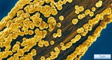 |
| New ultra-thin saw wire for cutting silicon wafers: diamond on top of carbon nanotubes. � Fraunhofer IWM |
Abstract:
More material could be saved when manufacturing wafers in future. Ultra-thin saws made of carbon nanotubes and diamond would be able to cut through silicon wafers with minimum kerf loss. A new method makes it possible to manufacture the saw wires.
Saws made of carbon
Freiburg, Germany | Posted on September 9th, 2013You can't saw without producing sawdust - and that can be expensive if, for example, the "dust" comes from wafer manufacturing in the photovoltaic and semiconductor industries, where relatively high kerf loss has been accepted as an unavoidable, if highly regrettable, fact of life. But now scientists from the Fraunhofer Institute for Mechanics of Materials IWM in Freiburg together with colleagues from the Australian Commonwealth Scientific and Industrial Research Organisation CSIRO have developed a saw wire that is set to effect dramatic reductions in kerf loss: in place of diamond-impregnated steel wires, the researchers use ultra-thin and extremely stable threads made of carbon nanotubes coated with diamond.
The potential of coated carbon nanotubes has long been understood: possible applications include its use as a hard and tough composite material or as a component of highly sensitive sensors and thermoelectric generators. However, the new material is extremely difficult to synthesize. Diamonds only grow under extreme conditions - at temperatures of around 900 degrees Celsius in an atmosphere containing hydrocarbons. Growing diamonds on nanotubes is a tricky proposition, because carbon tends to form graphite. In order to catalyse the formation of the diamond phase, it's necessary to use reactive hydrogen to prohibit the deposition of graphite. However, this process also damages the carbon nanotubes.
But the IWM scientist Manuel Mee found a solution for protecting the fine carbon nanotubes, which grow like forests on a substrate: "During our first experiments, fused silica from the reaction chamber accidentally came into contact with the coating plasma. It settled on the substrate and protected it against the aggressive hydrogen." And to his surprise, diamonds actually grew on this layer. "What followed was careful, painstaking work," points out Mee. "We had to study the silicon oxide layer, which was deposited in an undefined manner, and find a method of controlling the deposition and optimizing the process." Tests with a transmission electron microscope at CSIRO's lab in Australia revealed that the nanotubes actually survived under their protective layer.
A German-Australian success story
How exactly to proceed from there was the question that now faced the scientists. If they found a way to coat with diamond the nanothreads that the CSIRO specialists make from nanotubes, these diamond-coated nanothreads could be used to manufacture ultra-thin saws capable of cutting through silicon wafers for instance. The Australian team at CSIRO is one of the principal global experts with the know-how to manufacture yarns from carbon nanotubes. The manufacturing process requires special carbon nanotube "forests", which can be extracted as an ultra-thin "felt" and twisted into a very thin yarn ten to twenty micrometers in diameter. In principle, this diamond-coated yarn is the ideal material on which to base a new generation of saws, which could be used in the solar industry for example. As Mee explains: "The new saw wires held out the promise of being far superior to traditional steel wires. Because of their high tensile strength, they can be manufactured much thinner than steel wires - and that means significantly less kerf loss."
In the meantime, the physicist has managed to implement his idea. A joint patent application by Fraunhofer and CSIRO has already been filed for the method and corresponding products. Mee and his colleagues are currently carrying out sawing tests. "To be able to show our partners in industry the potential the technology holds," says Mee, "we have to demonstrate how it can help solar companies to save material when processing wafers."
####
For more information, please click here
Contacts:
Manuel Mee
49-761-514-2490
Copyright © Fraunhofer-Gesellschaft
If you have a comment, please Contact us.Issuers of news releases, not 7th Wave, Inc. or Nanotechnology Now, are solely responsible for the accuracy of the content.
Bookmark:


| Related Links |
![]() Research News August 2013 Complete Issue [ PDF 0.4399080276489258 MB ]:
Research News August 2013 Complete Issue [ PDF 0.4399080276489258 MB ]:
| Related News Press |
News and information
![]() Quantum computer improves AI predictions April 17th, 2026
Quantum computer improves AI predictions April 17th, 2026
![]() Flexible sensor gains sensitivity under pressure April 17th, 2026
Flexible sensor gains sensitivity under pressure April 17th, 2026
![]() A reusable chip for particulate matter sensing April 17th, 2026
A reusable chip for particulate matter sensing April 17th, 2026
![]() Detecting vibrational quantum beating in the predissociation dynamics of SF6 using time-resolved photoelectron spectroscopy April 17th, 2026
Detecting vibrational quantum beating in the predissociation dynamics of SF6 using time-resolved photoelectron spectroscopy April 17th, 2026
Chip Technology
![]() A reusable chip for particulate matter sensing April 17th, 2026
A reusable chip for particulate matter sensing April 17th, 2026
![]() Metasurfaces smooth light to boost magnetic sensing precision January 30th, 2026
Metasurfaces smooth light to boost magnetic sensing precision January 30th, 2026
Nanotubes/Buckyballs/Fullerenes/Nanorods/Nanostrings/Nanosheets
![]() Tiny nanosheets, big leap: A new sensor detects ethanol at ultra-low levels January 30th, 2026
Tiny nanosheets, big leap: A new sensor detects ethanol at ultra-low levels January 30th, 2026
![]() Enhancing power factor of p- and n-type single-walled carbon nanotubes April 25th, 2025
Enhancing power factor of p- and n-type single-walled carbon nanotubes April 25th, 2025
![]() Chainmail-like material could be the future of armor: First 2D mechanically interlocked polymer exhibits exceptional flexibility and strength January 17th, 2025
Chainmail-like material could be the future of armor: First 2D mechanically interlocked polymer exhibits exceptional flexibility and strength January 17th, 2025
![]() Innovative biomimetic superhydrophobic coating combines repair and buffering properties for superior anti-erosion December 13th, 2024
Innovative biomimetic superhydrophobic coating combines repair and buffering properties for superior anti-erosion December 13th, 2024
Discoveries
![]() Quantum computer improves AI predictions April 17th, 2026
Quantum computer improves AI predictions April 17th, 2026
![]() Flexible sensor gains sensitivity under pressure April 17th, 2026
Flexible sensor gains sensitivity under pressure April 17th, 2026
![]() A reusable chip for particulate matter sensing April 17th, 2026
A reusable chip for particulate matter sensing April 17th, 2026
![]() Detecting vibrational quantum beating in the predissociation dynamics of SF6 using time-resolved photoelectron spectroscopy April 17th, 2026
Detecting vibrational quantum beating in the predissociation dynamics of SF6 using time-resolved photoelectron spectroscopy April 17th, 2026
Materials/Metamaterials/Magnetoresistance
![]() First real-time observation of two-dimensional melting process: Researchers at Mainz University unveil new insights into magnetic vortex structures August 8th, 2025
First real-time observation of two-dimensional melting process: Researchers at Mainz University unveil new insights into magnetic vortex structures August 8th, 2025
![]() Researchers unveil a groundbreaking clay-based solution to capture carbon dioxide and combat climate change June 6th, 2025
Researchers unveil a groundbreaking clay-based solution to capture carbon dioxide and combat climate change June 6th, 2025
![]() A 1960s idea inspires NBI researchers to study hitherto inaccessible quantum states June 6th, 2025
A 1960s idea inspires NBI researchers to study hitherto inaccessible quantum states June 6th, 2025
![]() Institute for Nanoscience hosts annual proposal planning meeting May 16th, 2025
Institute for Nanoscience hosts annual proposal planning meeting May 16th, 2025
Announcements
![]() A fundamentally new therapeutic approach to cystic fibrosis: Nanobody repairs cellular defect April 17th, 2026
A fundamentally new therapeutic approach to cystic fibrosis: Nanobody repairs cellular defect April 17th, 2026
![]() UC Irvine physicists discover method to reverse �quantum scrambling� : The work addresses the problem of information loss in quantum computing system April 17th, 2026
UC Irvine physicists discover method to reverse �quantum scrambling� : The work addresses the problem of information loss in quantum computing system April 17th, 2026
Interviews/Book Reviews/Essays/Reports/Podcasts/Journals/White papers/Posters
![]() A fundamentally new therapeutic approach to cystic fibrosis: Nanobody repairs cellular defect April 17th, 2026
A fundamentally new therapeutic approach to cystic fibrosis: Nanobody repairs cellular defect April 17th, 2026
![]() UC Irvine physicists discover method to reverse �quantum scrambling� : The work addresses the problem of information loss in quantum computing system April 17th, 2026
UC Irvine physicists discover method to reverse �quantum scrambling� : The work addresses the problem of information loss in quantum computing system April 17th, 2026
Energy
![]() Sensors innovations for smart lithium-based batteries: advancements, opportunities, and potential challenges August 8th, 2025
Sensors innovations for smart lithium-based batteries: advancements, opportunities, and potential challenges August 8th, 2025
![]() Simple algorithm paired with standard imaging tool could predict failure in lithium metal batteries August 8th, 2025
Simple algorithm paired with standard imaging tool could predict failure in lithium metal batteries August 8th, 2025
Research partnerships
![]() Lab to industry: InSe wafer-scale breakthrough for future electronics August 8th, 2025
Lab to industry: InSe wafer-scale breakthrough for future electronics August 8th, 2025
![]() HKU physicists uncover hidden order in the quantum world through deconfined quantum critical points April 25th, 2025
HKU physicists uncover hidden order in the quantum world through deconfined quantum critical points April 25th, 2025
Solar/Photovoltaic
![]() Spinel-type sulfide semiconductors to operate the next-generation LEDs and solar cells For solar-cell absorbers and green-LED source October 3rd, 2025
Spinel-type sulfide semiconductors to operate the next-generation LEDs and solar cells For solar-cell absorbers and green-LED source October 3rd, 2025
![]() KAIST researchers introduce new and improved, next-generation perovskite solar cell November 8th, 2024
KAIST researchers introduce new and improved, next-generation perovskite solar cell November 8th, 2024
![]() Groundbreaking precision in single-molecule optoelectronics August 16th, 2024
Groundbreaking precision in single-molecule optoelectronics August 16th, 2024
![]() Development of zinc oxide nanopagoda array photoelectrode: photoelectrochemical water-splitting hydrogen production January 12th, 2024
Development of zinc oxide nanopagoda array photoelectrode: photoelectrochemical water-splitting hydrogen production January 12th, 2024
|
|
||
|
|
||
| The latest news from around the world, FREE | ||
|
|
||
|
|
||
| Premium Products | ||
|
|
||
|
Only the news you want to read!
Learn More |
||
|
|
||
|
Full-service, expert consulting
Learn More |
||
|
|
||