Home > Press > World's first large(wafer)-scale production of III-V semiconductor nanowire
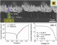 |
| This is an electrical characterization of the heterojunction solar cells composed of n- InAs0.7P0.3 nanowire array on p-Si (111) substrate.
Credit: UNIST |
Abstract:
The research team demonstrated a novel method to epitaxially synthesize structurally and compositionally homogeneous and spatially uniform ternary InAsyP1-y nanowire on Si at wafer-scale using metal-organic chemical vapor deposition (MOCVD). The high quality of the nanowires is reflected in the remarkably narrow PL and X-ray peak width and extremely low ideality factor in the InAsyP1-y nanowire/Si diode.
World's first large(wafer)-scale production of III-V semiconductor nanowire
Ulsan, South Korea | Posted on June 10th, 2013A nanowire is a nanostructure with a diameter of the order of a nanometer (10-9 meters). Alternatively, nanowires can be defined as structures that have a thickness or diameter constrained to tens of nanometers or less and an unconstrained length. Technology related to nanowires has been selected as one of the 10 Breakthrough Technologies of 2004 by MIT Technology Review.
High-aspect-ratio semiconductors have led to significant breakthroughs in conventional electrical, optical, and energy harvesting devices. Among such structures, III-V semiconductor nanowires offer unique properties arising from their high electron mobility and absorption coefficients, as well as their direct bandgaps.
A common technique for creating a nanowire is Vapor-Liquid-Solid (VLS) synthesis. This process can produce crystalline nanowires of some semiconductor materials. However, metal catalysts, usually expensive noble metals, should be used for initiating the VLS mechanism. In addition, these metal catalysts are known to significantly degrade the quality of semiconductor nanowires by creating deep levels, thus limiting practical applications of nanowires into opto-electronic devices.
In this work, however, Prof. Choi's group developed a novel technique of growing III-V semiconductor nanowires without metal catalysts or nano-patterning. Metal-organic chemical vapor deposition (MOCVD, AIXTRON A200) was used for the growth of the InAsyP1-y. 2 inch Si (111) wafer was cleaned with buffer oxide etch for 1 minute and deionized (DI) water for 2 seconds. Then, the wafer was immediately dipped in poly-L-lysine solution (Sigma-Aldrich inc.) for 3 minutes then rinsed in DI water for 10 seconds. The Si substrate was then loaded into the MOCVD reactor without any delay. The reactor pressure was lowered to 50 mbar with 15liter/min of hydrogen gas flow. Then the reactor was heated to growth temperatures (570 - 630 ℃), and stabilized for 10 minutes.
Kyoung Jin Choi, Associate Professor at Ulsan National Institute of Science and Technology (UNIST), Korea, and Xiuling Li, Professor at University of Illinois, U.S.A. led the research and this description of the new research was published on the web on May 7 in ACS Nano. (Title: Wafer-Scale Production of Uniform InAsyP1-y Nanowire Array on Silicon for Heterogeneous Integration).
"If we develop new technology which manages the density of nanowire and bandgap energy with further study, it is also possible to produce high-efficiency & low-cost large scale solar cells," said Prof. Choi. "This technology will give us a chance to lead the research on the new renewable energy."
This work was supported by the Future-based Technology Development Program (Nano Fields) through the National Research Foundation of Korea (NRF) funded by the Ministry of Education, Science and Technology.
####
For more information, please click here
Contacts:
Eunhee Song
82-522-171-224
Copyright © Ulsan National Institute of Science and Technology(UNIST)
If you have a comment, please Contact us.Issuers of news releases, not 7th Wave, Inc. or Nanotechnology Now, are solely responsible for the accuracy of the content.
Bookmark:


| Related News Press |
News and information
![]() Quantum computer improves AI predictions April 17th, 2026
Quantum computer improves AI predictions April 17th, 2026
![]() Flexible sensor gains sensitivity under pressure April 17th, 2026
Flexible sensor gains sensitivity under pressure April 17th, 2026
![]() A reusable chip for particulate matter sensing April 17th, 2026
A reusable chip for particulate matter sensing April 17th, 2026
![]() Detecting vibrational quantum beating in the predissociation dynamics of SF6 using time-resolved photoelectron spectroscopy April 17th, 2026
Detecting vibrational quantum beating in the predissociation dynamics of SF6 using time-resolved photoelectron spectroscopy April 17th, 2026
Govt.-Legislation/Regulation/Funding/Policy
![]() Quantum computer improves AI predictions April 17th, 2026
Quantum computer improves AI predictions April 17th, 2026
![]() Metasurfaces smooth light to boost magnetic sensing precision January 30th, 2026
Metasurfaces smooth light to boost magnetic sensing precision January 30th, 2026
![]() New imaging approach transforms study of bacterial biofilms August 8th, 2025
New imaging approach transforms study of bacterial biofilms August 8th, 2025
Chip Technology
![]() A reusable chip for particulate matter sensing April 17th, 2026
A reusable chip for particulate matter sensing April 17th, 2026
![]() Metasurfaces smooth light to boost magnetic sensing precision January 30th, 2026
Metasurfaces smooth light to boost magnetic sensing precision January 30th, 2026
Nanoelectronics
![]() Lab to industry: InSe wafer-scale breakthrough for future electronics August 8th, 2025
Lab to industry: InSe wafer-scale breakthrough for future electronics August 8th, 2025
![]() Interdisciplinary: Rice team tackles the future of semiconductors Multiferroics could be the key to ultralow-energy computing October 6th, 2023
Interdisciplinary: Rice team tackles the future of semiconductors Multiferroics could be the key to ultralow-energy computing October 6th, 2023
![]() Key element for a scalable quantum computer: Physicists from Forschungszentrum J�lich and RWTH Aachen University demonstrate electron transport on a quantum chip September 23rd, 2022
Key element for a scalable quantum computer: Physicists from Forschungszentrum J�lich and RWTH Aachen University demonstrate electron transport on a quantum chip September 23rd, 2022
![]() Reduced power consumption in semiconductor devices September 23rd, 2022
Reduced power consumption in semiconductor devices September 23rd, 2022
Discoveries
![]() Quantum computer improves AI predictions April 17th, 2026
Quantum computer improves AI predictions April 17th, 2026
![]() Flexible sensor gains sensitivity under pressure April 17th, 2026
Flexible sensor gains sensitivity under pressure April 17th, 2026
![]() A reusable chip for particulate matter sensing April 17th, 2026
A reusable chip for particulate matter sensing April 17th, 2026
![]() Detecting vibrational quantum beating in the predissociation dynamics of SF6 using time-resolved photoelectron spectroscopy April 17th, 2026
Detecting vibrational quantum beating in the predissociation dynamics of SF6 using time-resolved photoelectron spectroscopy April 17th, 2026
Announcements
![]() A fundamentally new therapeutic approach to cystic fibrosis: Nanobody repairs cellular defect April 17th, 2026
A fundamentally new therapeutic approach to cystic fibrosis: Nanobody repairs cellular defect April 17th, 2026
![]() UC Irvine physicists discover method to reverse �quantum scrambling� : The work addresses the problem of information loss in quantum computing system April 17th, 2026
UC Irvine physicists discover method to reverse �quantum scrambling� : The work addresses the problem of information loss in quantum computing system April 17th, 2026
Research partnerships
![]() Lab to industry: InSe wafer-scale breakthrough for future electronics August 8th, 2025
Lab to industry: InSe wafer-scale breakthrough for future electronics August 8th, 2025
![]() HKU physicists uncover hidden order in the quantum world through deconfined quantum critical points April 25th, 2025
HKU physicists uncover hidden order in the quantum world through deconfined quantum critical points April 25th, 2025
|
|
||
|
|
||
| The latest news from around the world, FREE | ||
|
|
||
|
|
||
| Premium Products | ||
|
|
||
|
Only the news you want to read!
Learn More |
||
|
|
||
|
Full-service, expert consulting
Learn More |
||
|
|
||