Home > Press > ORNL microscopy uncovers "dancing" silicon atoms in graphene
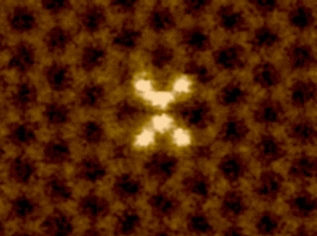 |
| Oak Ridge National Laboratory researchers used electron microscopy to document the 'dancing' motions of silicon atoms, pictured in white, in a graphene sheet. |
Abstract:
Jumping silicon atoms are the stars of an atomic scale ballet featured in a new Nature Communications study from the Department of Energy's Oak Ridge National Laboratory.
ORNL microscopy uncovers "dancing" silicon atoms in graphene
Oak Ridge, TN | Posted on April 4th, 2013 The ORNL research team documented the atoms' unique behavior by first trapping groups of silicon atoms, known as clusters, in a single-atom-thick sheet of carbon called graphene. The silicon clusters, composed of six atoms, were pinned in place by pores in the graphene sheet, allowing the team to directly image the material with a scanning transmission electron microscope.
The "dancing" movement of the silicon atoms, seen in a video here: http://www.ornl.gov/ornlhome/video/video_files/dancing-silicons-1.mov, was caused by the energy transferred to the material from the electron beam of the team's microscope.
"It's not the first time people have seen clusters of silicon," said coauthor Juan Carlos Idrobo. "The problem is when you put an electron beam on them, you insert energy into the cluster and make the atoms move around. The difference with these results is that the change that we observed was reversible. We were able to see how the silicon cluster changes its structure back and forth by having one of its atoms 'dancing' between two different positions."
Other techniques to study clusters are indirect, says Jaekwang Lee, first author on the ORNL study. "With the conventional instrumentation used to study clusters, it is not yet possible to directly identify the three-dimensional atomic structure of the cluster," Lee said.
The ability to analyze the structure of small clusters is important for scientists because this insight can be used to precisely understand how different atomic configurations control a material's properties. Molecules could then be tailored for specific uses.
"Capturing atomic clusters inside patterned graphene nanopores could potentially lead to practical applications in areas such as electronic and optoelectronic devices, as well as catalysis," Lee said. "It would be a new approach to tuning electronic and optical properties in materials."
The ORNL team confirmed its experimental findings with theoretical calculations, which helped explain how much energy was required for the silicon atom to switch back and forth between different positions.
This research was supported by National Science Foundation, DOE's Office of Science, the McMinn Endowment at Vanderbilt University, and by DOE's Office of Science User Facilities: ORNL's Shared Research Equipment User Facility Program and the National Energy Research Scientific Computing Center at Lawrence Berkeley National Laboratory.
####
About Oak Ridge National Laboratory
ORNL is managed by UT-Battelle for the Department of Energy's Office of Science. DOE's Office of Science is the single largest supporter of basic research in the physical sciences in the United States, and is working to address some of the most pressing challenges of our time. For more information, please visit science.energy.gov.
For more information, please click here
Contacts:
Morgan McCorkle
Communications and Media Relations
865.574.7308
Copyright © Oak Ridge National Laboratory
If you have a comment, please Contact us.Issuers of news releases, not 7th Wave, Inc. or Nanotechnology Now, are solely responsible for the accuracy of the content.
Bookmark:


| Related Links |
| Related News Press |
News and information
![]() Quantum computer improves AI predictions April 17th, 2026
Quantum computer improves AI predictions April 17th, 2026
![]() Flexible sensor gains sensitivity under pressure April 17th, 2026
Flexible sensor gains sensitivity under pressure April 17th, 2026
![]() A reusable chip for particulate matter sensing April 17th, 2026
A reusable chip for particulate matter sensing April 17th, 2026
![]() Detecting vibrational quantum beating in the predissociation dynamics of SF6 using time-resolved photoelectron spectroscopy April 17th, 2026
Detecting vibrational quantum beating in the predissociation dynamics of SF6 using time-resolved photoelectron spectroscopy April 17th, 2026
Laboratories
![]() Researchers develop molecular qubits that communicate at telecom frequencies October 3rd, 2025
Researchers develop molecular qubits that communicate at telecom frequencies October 3rd, 2025
Graphene/ Graphite
![]() Electrifying results shed light on graphene foam as a potential material for lab grown cartilage June 6th, 2025
Electrifying results shed light on graphene foam as a potential material for lab grown cartilage June 6th, 2025
![]() Breakthrough in proton barrier films using pore-free graphene oxide: Kumamoto University researchers achieve new milestone in advanced coating technologies September 13th, 2024
Breakthrough in proton barrier films using pore-free graphene oxide: Kumamoto University researchers achieve new milestone in advanced coating technologies September 13th, 2024
Govt.-Legislation/Regulation/Funding/Policy
![]() Quantum computer improves AI predictions April 17th, 2026
Quantum computer improves AI predictions April 17th, 2026
![]() Metasurfaces smooth light to boost magnetic sensing precision January 30th, 2026
Metasurfaces smooth light to boost magnetic sensing precision January 30th, 2026
![]() New imaging approach transforms study of bacterial biofilms August 8th, 2025
New imaging approach transforms study of bacterial biofilms August 8th, 2025
Discoveries
![]() Quantum computer improves AI predictions April 17th, 2026
Quantum computer improves AI predictions April 17th, 2026
![]() Flexible sensor gains sensitivity under pressure April 17th, 2026
Flexible sensor gains sensitivity under pressure April 17th, 2026
![]() A reusable chip for particulate matter sensing April 17th, 2026
A reusable chip for particulate matter sensing April 17th, 2026
![]() Detecting vibrational quantum beating in the predissociation dynamics of SF6 using time-resolved photoelectron spectroscopy April 17th, 2026
Detecting vibrational quantum beating in the predissociation dynamics of SF6 using time-resolved photoelectron spectroscopy April 17th, 2026
Announcements
![]() A fundamentally new therapeutic approach to cystic fibrosis: Nanobody repairs cellular defect April 17th, 2026
A fundamentally new therapeutic approach to cystic fibrosis: Nanobody repairs cellular defect April 17th, 2026
![]() UC Irvine physicists discover method to reverse �quantum scrambling� : The work addresses the problem of information loss in quantum computing system April 17th, 2026
UC Irvine physicists discover method to reverse �quantum scrambling� : The work addresses the problem of information loss in quantum computing system April 17th, 2026
Research partnerships
![]() Lab to industry: InSe wafer-scale breakthrough for future electronics August 8th, 2025
Lab to industry: InSe wafer-scale breakthrough for future electronics August 8th, 2025
![]() HKU physicists uncover hidden order in the quantum world through deconfined quantum critical points April 25th, 2025
HKU physicists uncover hidden order in the quantum world through deconfined quantum critical points April 25th, 2025
|
|
||
|
|
||
| The latest news from around the world, FREE | ||
|
|
||
|
|
||
| Premium Products | ||
|
|
||
|
Only the news you want to read!
Learn More |
||
|
|
||
|
Full-service, expert consulting
Learn More |
||
|
|
||