Home > Press > Argonne licenses diamond semiconductor discoveries to AKHAN Technologies
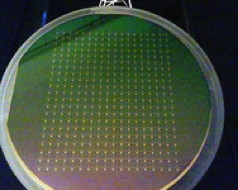 |
| This wafer of nanocrystalline diamond provides one example of the technology that AKHAN Technologies has licensed from Argonne. To view a larger version of the image, click on it. Photo courtesy Ani Sumant. |
Abstract:
he U.S. Department of Energy's Argonne National Laboratory announced today that the laboratory has granted AKHAN Technologies exclusive diamond semiconductor application licensing rights to breakthrough low-temperature diamond deposition technology developed by Argonne's Center for Nanoscale Materials (CNM).
Argonne licenses diamond semiconductor discoveries to AKHAN Technologies
Lemont, IL | Posted on March 7th, 2013The Argonne-developed technology allows for the deposition of nanocrystalline diamond on a variety of wafer substrate materials at temperatures as low as 400 degrees Celsius. The combination of the Argonne's low-temperature diamond technology with AKHAN's Miraj Diamond� process represents the state of the art in diamond semiconductor thin-film technology.
"This licensing agreement gives us the impact of a one-two punch, in which we combine AKHAN's novel process to achieve efficient n-type doping in diamond with Argonne's low-temperature diamond deposition technology," said Argonne nanoscientist Anirudha Sumant. "This will break barriers that restricted the use of diamond thin films in the semiconductor industry limited to only p-type doping."
"This is an important step in the realization of a �Diamond Age,'" added Andreas Roelofs, Argonne's CNM Deputy Division Director and Industrial Relations Liaison. "It is always wonderful to see when basic materials research leads to promising new technology developments. Having a company license your technology is the best proof of showing that you are working on relevant questions."
AKHAN and Argonne are planning to develop this further through a Cooperative Research and Development Agreement (CRADA) initiative.
As part of a recent collaborative project, AKHAN and Argonne researchers were able to demonstrate working diamond devices with improved performance using the Miraj Diamond� process based on conventional high temperature nanocrystalline diamond. AKHAN announced the availability of published characterization data of the company's Miraj Diamond� technology in the Materials Research Society (MRS) Online Proceedings Library. In the paper, titled "On Enabling Nanocrystalline Diamond For Device Use: Novel Ion Beam Methodology and The Realization Of Shallow N-Type Diamond," AKHAN and Argonne researchers confirm breakthrough morphological, phase, and electrical characterization data for both n-type NCD wafer material and NCD PIN diode devices. The full paper is available through Cambridge Journals Online.
After many years of research and development, AKHAN Technologies, Inc., an Illinois Company, was formed in April 2007 by its founder, Adam Khan, to commercialize Diamond Lattice Technology. Commercial realization of diamond-based electron devices is the primary focus of AKHAN Technologies, Inc. Further, AKHAN Technologies, Inc., is committed to continually introducing the most advanced diamond device technology in both the digital and discrete markets to the global semiconductor community. With extensive diamond technology experience and a strong Board of Directors, AKHAN is well positioned to play an important role in enabling the "diamond age" of microelectronics. For more information, please visit the AKHAN Technologies website.
####
About Argonne National Laboratory
Argonne National Laboratory seeks solutions to pressing national problems in science and technology. The nation's first national laboratory, Argonne conducts leading-edge basic and applied scientific research in virtually every scientific discipline. Argonne researchers work closely with researchers from hundreds of companies, universities, and federal, state and municipal agencies to help them solve their specific problems, advance America's scientific leadership and prepare the nation for a better future. With employees from more than 60 nations, Argonne is managed by UChicago Argonne, LLC for the U.S. Department of Energy's Office of Science.
The Center for Nanoscale Materials at Argonne National Laboratory is one of the five DOE Nanoscale Science Research Centers (NSRCs), which are premier national user facilities for interdisciplinary research at the nanoscale and are supported by the DOE Office of Science. Together, the NSRCs comprise a suite of complementary facilities that provide researchers with state-of-the-art capabilities to fabricate, process, characterize and model nanoscale materials. The NSRCs constitute the largest infrastructure investment of the National Nanotechnology Initiative, and they are located at DOE�s Argonne, Brookhaven, Lawrence Berkeley, Oak Ridge, Sandia and Los Alamos National Laboratories. For more information about the DOE NSRCs, please visit www.nano.gov.
For more information, please click here
Contacts:
Jared Sagoff
(630) 252-5549
Copyright © Argonne National Laboratory
If you have a comment, please Contact us.Issuers of news releases, not 7th Wave, Inc. or Nanotechnology Now, are solely responsible for the accuracy of the content.
Bookmark:


| Related News Press |
News and information
![]() Quantum computer improves AI predictions April 17th, 2026
Quantum computer improves AI predictions April 17th, 2026
![]() Flexible sensor gains sensitivity under pressure April 17th, 2026
Flexible sensor gains sensitivity under pressure April 17th, 2026
![]() A reusable chip for particulate matter sensing April 17th, 2026
A reusable chip for particulate matter sensing April 17th, 2026
![]() Detecting vibrational quantum beating in the predissociation dynamics of SF6 using time-resolved photoelectron spectroscopy April 17th, 2026
Detecting vibrational quantum beating in the predissociation dynamics of SF6 using time-resolved photoelectron spectroscopy April 17th, 2026
Thin films
![]() Tiny nanosheets, big leap: A new sensor detects ethanol at ultra-low levels January 30th, 2026
Tiny nanosheets, big leap: A new sensor detects ethanol at ultra-low levels January 30th, 2026
![]() Utilizing palladium for addressing contact issues of buried oxide thin film transistors April 5th, 2024
Utilizing palladium for addressing contact issues of buried oxide thin film transistors April 5th, 2024
Laboratories
![]() Researchers develop molecular qubits that communicate at telecom frequencies October 3rd, 2025
Researchers develop molecular qubits that communicate at telecom frequencies October 3rd, 2025
Govt.-Legislation/Regulation/Funding/Policy
![]() Quantum computer improves AI predictions April 17th, 2026
Quantum computer improves AI predictions April 17th, 2026
![]() Metasurfaces smooth light to boost magnetic sensing precision January 30th, 2026
Metasurfaces smooth light to boost magnetic sensing precision January 30th, 2026
![]() New imaging approach transforms study of bacterial biofilms August 8th, 2025
New imaging approach transforms study of bacterial biofilms August 8th, 2025
Chip Technology
![]() A reusable chip for particulate matter sensing April 17th, 2026
A reusable chip for particulate matter sensing April 17th, 2026
![]() Metasurfaces smooth light to boost magnetic sensing precision January 30th, 2026
Metasurfaces smooth light to boost magnetic sensing precision January 30th, 2026
Announcements
![]() A fundamentally new therapeutic approach to cystic fibrosis: Nanobody repairs cellular defect April 17th, 2026
A fundamentally new therapeutic approach to cystic fibrosis: Nanobody repairs cellular defect April 17th, 2026
![]() UC Irvine physicists discover method to reverse �quantum scrambling� : The work addresses the problem of information loss in quantum computing system April 17th, 2026
UC Irvine physicists discover method to reverse �quantum scrambling� : The work addresses the problem of information loss in quantum computing system April 17th, 2026
Patents/IP/Tech Transfer/Licensing
![]() Getting drugs across the blood-brain barrier using nanoparticles March 3rd, 2023
Getting drugs across the blood-brain barrier using nanoparticles March 3rd, 2023
![]() Metasurfaces control polarized light at will: New research unlocks the hidden potential of metasurfaces August 13th, 2021
Metasurfaces control polarized light at will: New research unlocks the hidden potential of metasurfaces August 13th, 2021
![]() Arrowhead Pharmaceuticals Announces Closing of Agreement with Takeda November 27th, 2020
Arrowhead Pharmaceuticals Announces Closing of Agreement with Takeda November 27th, 2020
|
|
||
|
|
||
| The latest news from around the world, FREE | ||
|
|
||
|
|
||
| Premium Products | ||
|
|
||
|
Only the news you want to read!
Learn More |
||
|
|
||
|
Full-service, expert consulting
Learn More |
||
|
|
||