Home > Press > New technique could improve optical devices
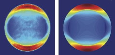 |
| The orientation of light emission The angular distribution of light emission from monolayer MoS2, left, closely matches the theoretical calculations for in-plane oriented emitters, right, indicating that light emission from MoS2 originates from in-plane oriented emitters. Credit: Zia lab/Brown University |
Abstract:
Understanding the source and orientation of light in light-emitting thin films — now possible with energy-momentum spectroscopy — could lead to better LEDs, solar cells, and other devices that use layered nanomaterials.
New technique could improve optical devices
Providence, RI | Posted on March 5th, 2013A multi-university research team has used a new spectroscopic method to gain a key insight into how light is emitted from layered nanomaterials and other thin films.
The technique, called energy-momentum spectroscopy, enables researchers to look at the light emerging from a thin film and determine whether it is coming from emitters oriented along the plane of the film or from emitters oriented perpendicular to the film. Knowing the orientations of emitters could help engineers make better use of thin-film materials in optical devices like LEDs or solar cells.
The research, published online on March 3 in Nature Nanotechnology, was a collaborative effort of Brown University, Case Western Reserve University, Columbia University, and the University of California-Santa Barbara.
The new technique takes advantage of a fundamental property of thin films: interference. Interference effects can be seen in the rainbow colors visible on the surface of soap bubbles or oil slicks. Scientists can analyze how light constructively and destructively interferes at different angles to draw conclusions about the film itself — how thick it is, for example. This new technique takes that kind of analysis one step further for light-emitting thin films.
"The key difference in our technique is we're looking at the energy as well as the angle and polarization at which light is emitted," said Rashid Zia, assistant professor of engineering at Brown University and one of the study's lead authors. "We can relate these different angles to distinct orientations of emitters in the film. At some angles and polarizations, we see only the light emission from in-plane emitters, while at other angles and polarizations we see only light originating from out-of-plane emitters."
The researchers demonstrated their technique on two important thin-film materials, molybdenum disulfide (MoS2) and PTCDA. Each represents a class of materials that shows promise for optical applications. MoS2 is a two-dimensional material similar to graphene, and PTCDA is an organic semiconductor. The research showed that light emission from MoS2 occurs only from in-plane emitters. In PTCDA, light comes from two distinct species of emitters, one in-plane and one out-of-plane.
####
About Brown University
Once the orientation of the emitters is known, Zia says, it may be possible to design structured devices that maximize those directional properties. In most applications, thin-film materials are layered on top of each other. The orientations of emitters in each layer indicate whether electronic excitations are happening within each layer or across layers, and that has implications for how such a device should be configured.
“If you were making an LED using these layered materials and you knew that the electronic excitations were happening across an interface,” Zia said, “then there’s a specific way you want to design the structure to get all of that light out and increase its overall efficiency.”
The same concept could apply to light-absorbing devices like solar cells. By understanding how the electronic excitations happen in the material, it could be possible to structure it in a way that coverts more incoming light to electricity.
“One of the exciting things about this research is how it brought together people with different expertise,” Zia said. “Our group’s expertise at Brown is in developing new forms of spectroscopy and studying the electronic origin of light emission. The Kymissis group at Columbia has a great deal of expertise in organic semiconductors, and the Shan group at Case Western has a great deal of expertise in layered nanomaterials. Jon Schuller, the study’s first author, did a great job in bringing all this expertise together. Jon was a visiting scientist here at Brown, a postdoctoral fellow in the Energy Frontier Research Center at Columbia, and is now a professor at UCSB.”
Other authors on the paper were Sinan Karaveli (Brown), Theanne Schiros (Columbia), Keliang He (Case Western), Shyuan Yang (Columbia), Ioannis Kymissis (Columbia) and Jie Shan (Case Western). Funding for the work was provided by the Air Force Office of Scientific Research, the Department of Energy, the National Science Foundation, and the Nanoelectronic Research Initiative of the Semiconductor Research Corporation.
For more information, please click here
Contacts:
Kevin Stacey
401-863-3766
Copyright © Brown University
If you have a comment, please Contact us.Issuers of news releases, not 7th Wave, Inc. or Nanotechnology Now, are solely responsible for the accuracy of the content.
Bookmark:


| Related News Press |
News and information
![]() Quantum computer improves AI predictions April 17th, 2026
Quantum computer improves AI predictions April 17th, 2026
![]() Flexible sensor gains sensitivity under pressure April 17th, 2026
Flexible sensor gains sensitivity under pressure April 17th, 2026
![]() A reusable chip for particulate matter sensing April 17th, 2026
A reusable chip for particulate matter sensing April 17th, 2026
![]() Detecting vibrational quantum beating in the predissociation dynamics of SF6 using time-resolved photoelectron spectroscopy April 17th, 2026
Detecting vibrational quantum beating in the predissociation dynamics of SF6 using time-resolved photoelectron spectroscopy April 17th, 2026
Thin films
![]() Tiny nanosheets, big leap: A new sensor detects ethanol at ultra-low levels January 30th, 2026
Tiny nanosheets, big leap: A new sensor detects ethanol at ultra-low levels January 30th, 2026
Display technology/LEDs/SS Lighting/OLEDs
![]() Spinel-type sulfide semiconductors to operate the next-generation LEDs and solar cells For solar-cell absorbers and green-LED source October 3rd, 2025
Spinel-type sulfide semiconductors to operate the next-generation LEDs and solar cells For solar-cell absorbers and green-LED source October 3rd, 2025
![]() Efficient and stable hybrid perovskite-organic light-emitting diodes with external quantum efficiency exceeding 40 per cent July 5th, 2024
Efficient and stable hybrid perovskite-organic light-emitting diodes with external quantum efficiency exceeding 40 per cent July 5th, 2024
Govt.-Legislation/Regulation/Funding/Policy
![]() Quantum computer improves AI predictions April 17th, 2026
Quantum computer improves AI predictions April 17th, 2026
![]() Metasurfaces smooth light to boost magnetic sensing precision January 30th, 2026
Metasurfaces smooth light to boost magnetic sensing precision January 30th, 2026
![]() New imaging approach transforms study of bacterial biofilms August 8th, 2025
New imaging approach transforms study of bacterial biofilms August 8th, 2025
Discoveries
![]() Quantum computer improves AI predictions April 17th, 2026
Quantum computer improves AI predictions April 17th, 2026
![]() Flexible sensor gains sensitivity under pressure April 17th, 2026
Flexible sensor gains sensitivity under pressure April 17th, 2026
![]() A reusable chip for particulate matter sensing April 17th, 2026
A reusable chip for particulate matter sensing April 17th, 2026
![]() Detecting vibrational quantum beating in the predissociation dynamics of SF6 using time-resolved photoelectron spectroscopy April 17th, 2026
Detecting vibrational quantum beating in the predissociation dynamics of SF6 using time-resolved photoelectron spectroscopy April 17th, 2026
Announcements
![]() A fundamentally new therapeutic approach to cystic fibrosis: Nanobody repairs cellular defect April 17th, 2026
A fundamentally new therapeutic approach to cystic fibrosis: Nanobody repairs cellular defect April 17th, 2026
![]() UC Irvine physicists discover method to reverse ‘quantum scrambling’ : The work addresses the problem of information loss in quantum computing system April 17th, 2026
UC Irvine physicists discover method to reverse ‘quantum scrambling’ : The work addresses the problem of information loss in quantum computing system April 17th, 2026
Tools
![]() Metasurfaces smooth light to boost magnetic sensing precision January 30th, 2026
Metasurfaces smooth light to boost magnetic sensing precision January 30th, 2026
![]() From sensors to smart systems: the rise of AI-driven photonic noses January 30th, 2026
From sensors to smart systems: the rise of AI-driven photonic noses January 30th, 2026
![]() Japan launches fully domestically produced quantum computer: Expo visitors to experience quantum computing firsthand August 8th, 2025
Japan launches fully domestically produced quantum computer: Expo visitors to experience quantum computing firsthand August 8th, 2025
Military
![]() Quantum engineers ‘squeeze’ laser frequency combs to make more sensitive gas sensors January 17th, 2025
Quantum engineers ‘squeeze’ laser frequency combs to make more sensitive gas sensors January 17th, 2025
![]() Chainmail-like material could be the future of armor: First 2D mechanically interlocked polymer exhibits exceptional flexibility and strength January 17th, 2025
Chainmail-like material could be the future of armor: First 2D mechanically interlocked polymer exhibits exceptional flexibility and strength January 17th, 2025
![]() Single atoms show their true color July 5th, 2024
Single atoms show their true color July 5th, 2024
![]() NRL charters Navy’s quantum inertial navigation path to reduce drift April 5th, 2024
NRL charters Navy’s quantum inertial navigation path to reduce drift April 5th, 2024
Energy
![]() Sensors innovations for smart lithium-based batteries: advancements, opportunities, and potential challenges August 8th, 2025
Sensors innovations for smart lithium-based batteries: advancements, opportunities, and potential challenges August 8th, 2025
![]() Simple algorithm paired with standard imaging tool could predict failure in lithium metal batteries August 8th, 2025
Simple algorithm paired with standard imaging tool could predict failure in lithium metal batteries August 8th, 2025
Grants/Sponsored Research/Awards/Scholarships/Gifts/Contests/Honors/Records
![]() Quantum computer improves AI predictions April 17th, 2026
Quantum computer improves AI predictions April 17th, 2026
![]() Detecting vibrational quantum beating in the predissociation dynamics of SF6 using time-resolved photoelectron spectroscopy April 17th, 2026
Detecting vibrational quantum beating in the predissociation dynamics of SF6 using time-resolved photoelectron spectroscopy April 17th, 2026
![]() Metasurfaces smooth light to boost magnetic sensing precision January 30th, 2026
Metasurfaces smooth light to boost magnetic sensing precision January 30th, 2026
Research partnerships
![]() Lab to industry: InSe wafer-scale breakthrough for future electronics August 8th, 2025
Lab to industry: InSe wafer-scale breakthrough for future electronics August 8th, 2025
![]() HKU physicists uncover hidden order in the quantum world through deconfined quantum critical points April 25th, 2025
HKU physicists uncover hidden order in the quantum world through deconfined quantum critical points April 25th, 2025
Solar/Photovoltaic
![]() Spinel-type sulfide semiconductors to operate the next-generation LEDs and solar cells For solar-cell absorbers and green-LED source October 3rd, 2025
Spinel-type sulfide semiconductors to operate the next-generation LEDs and solar cells For solar-cell absorbers and green-LED source October 3rd, 2025
![]() KAIST researchers introduce new and improved, next-generation perovskite solar cell November 8th, 2024
KAIST researchers introduce new and improved, next-generation perovskite solar cell November 8th, 2024
![]() Groundbreaking precision in single-molecule optoelectronics August 16th, 2024
Groundbreaking precision in single-molecule optoelectronics August 16th, 2024
![]() Development of zinc oxide nanopagoda array photoelectrode: photoelectrochemical water-splitting hydrogen production January 12th, 2024
Development of zinc oxide nanopagoda array photoelectrode: photoelectrochemical water-splitting hydrogen production January 12th, 2024
|
|
||
|
|
||
| The latest news from around the world, FREE | ||
|
|
||
|
|
||
| Premium Products | ||
|
|
||
|
Only the news you want to read!
Learn More |
||
|
|
||
|
Full-service, expert consulting
Learn More |
||
|
|
||