Home > Press > The world's most sensitive plasmon resonance sensor inspired by ancient Roman cup: World's most sensitive plasmon resonance sensor
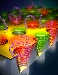 |
| This image shows a model of nano cup arrays.
Credit: University of Illinois at Urbana-Champaign |
Abstract:
Utilizing optical characteristics first demonstrated by the ancient Romans, researchers at the University of Illinois at Urbana-Champaign have created a novel, ultra-sensitive tool for chemical, DNA, and protein analysis.
The world's most sensitive plasmon resonance sensor inspired by ancient Roman cup: World's most sensitive plasmon resonance sensor
Urbana, IL | Posted on February 14th, 2013"With this device, the nanoplasmonic spectroscopy sensing, for the first time, becomes colorimetric sensing, requiring only naked eyes or ordinary visible color photography," explained Logan Liu, an assistant professor of electrical and computer engineering and of bioengineering at Illinois. "It can be used for chemical imaging, biomolecular imaging, and integration to portable microfluidics devices for lab-on-chip-applications. His research team's results were featured in the cover article of the inaugural edition of Advanced Optical Materials (AOM, optical section of Advanced Materials).
The Lycurgus cup was created by the Romans in 400 A.D. Made of a dichroic glass, the famous cup exhibits different colors depending on whether or not light is passing through it; red when lit from behind and green when lit from in front. It is also the origin of inspiration for all contemporary nanoplasmonics research�the study of optical phenomena in the nanoscale vicinity of metal surfaces.
"This dichroic effect was achieved by including tiny proportions of minutely ground gold and silver dust in the glass," Liu added. "In our research, we have created a large-area high density array of a nanoscale Lycurgus cup using a transparent plastic substrate to achieve colorimetric sensing. The sensor consists of about one billion nano cups in an array with sub-wavelength opening and decorated with metal nanoparticles on side walls, having similar shape and properties as the Lycurgus cups displayed in a British museum. Liu and his team were particularly excited by the extraordinary characteristics of the material, yielding 100 times better sensitivity than any other reported nanoplasmonic device.
Colorimetric techniques are mainly attractive because of their low cost, use of inexpensive equipment, requirement of fewer signal transduction hardware, and above all, providing simple-to-understand results. Colorimetric sensor can be used for both qualitative analytic identification as well as quantitative analysis. The current design will also enable new technology development in the field of DNA/protein microarray.
"Our label-free colorimetric sensor eliminates the need of problematic fluorescence tagging of DNA/ protein molecules, and the hybridization of probe and target molecule is detected from the color change of the sensor," stated Manas Gartia, first author of the article, "Colorimetrics: Colorimetric Plasmon Resonance Imaging Using Nano Lycurgus Cup Arrays." "Our current sensor requires just a light source and a camera to complete the DNA sensing process. This opens the possibility for developing affordable, simple and sensitive mobile phone-based DNA microarray detector in near future. Due to its low cost, simplicity in design, and high sensitivity, we envisage the extensive use of the device for DNA microarrays, therapeutic antibody screening for drug discovery, and pathogen detection in resource poor setting."
Gartia explained that light-matter interaction using sub-wavelength hole arrays gives rise to interesting optical phenomena such as surface plasmon polaritons (SPPs) mediated enhanced optical transmission (EOT). In case of EOT, more than expected amount of light can be transmitted through nanoholes on otherwise opaque metal thin films. Since the thin metal film has special optical property called surface plasmon resonance (SPR) which is affected by tiny amount surrounding materials, such device has been used as biosensing applications.
According to the researchers, most of the previous studies have mainly focused on manipulating in-plane two-dimensional (2D) EOT structures such as tuning the hole diameter, shape, or distance between the holes. In addition, most of the previous studies are concerned with straight holes only. Here, the EOT is mediated mainly by SPPs, which limits the sensitivity and figure of merits obtainable from such devices.
"Our current design employs 3D sub-wavelength tapered periodic hole array plasmonic structure. In contrast to the SPP mediated EOT, the proposed structure relies on Localized Surface Plasmon (LSP) mediated EOT," Gartia said. "The advantage of LSPs is that the enhanced transmission at different wavelengths and with different dispersion properties can be tuned by controlling the size, shape, and materials of the 3D holes. The tapered geometry will funnel and adiabatically focus the photons on to the sub-wavelength plasmonic structure at the bottom, leading to large local electric field and enhancement of EOT.
"Secondly the localized resonance supported by 3D plasmonic structure will enable broadband tuning of optical transmission through controlling the shape, size, and period of holes as well as the shape, size, and period of metallic particles decorated at the side walls. In other words, we will have more controllability over tuning the resonance wavelengths of the sensor."
In addition to Gartia and Liu, the paper's co-authors included Austin Hsiao, Anusha Pokhriyal, Sujin Seo, Gulsim Kulsharova, and Brian T. Cunningham at Illinois, and Tiziana C. Bond, at the Meso, Micro and Nano Technologies Center at Lawrence Livermore National Laboratory, California.
####
For more information, please click here
Contacts:
Logan Liu
217-244-4349
Copyright © University of Illinois College of Engineering
If you have a comment, please Contact us.Issuers of news releases, not 7th Wave, Inc. or Nanotechnology Now, are solely responsible for the accuracy of the content.
Bookmark:


| Related News Press |
Imaging
![]() Simple algorithm paired with standard imaging tool could predict failure in lithium metal batteries August 8th, 2025
Simple algorithm paired with standard imaging tool could predict failure in lithium metal batteries August 8th, 2025
![]() First real-time observation of two-dimensional melting process: Researchers at Mainz University unveil new insights into magnetic vortex structures August 8th, 2025
First real-time observation of two-dimensional melting process: Researchers at Mainz University unveil new insights into magnetic vortex structures August 8th, 2025
![]() New imaging approach transforms study of bacterial biofilms August 8th, 2025
New imaging approach transforms study of bacterial biofilms August 8th, 2025
Microfluidics/Nanofluidics
![]() Projecting light to dispense liquids: A new route to ultra-precise microdroplets January 30th, 2026
Projecting light to dispense liquids: A new route to ultra-precise microdroplets January 30th, 2026
Laboratories
![]() Researchers develop molecular qubits that communicate at telecom frequencies October 3rd, 2025
Researchers develop molecular qubits that communicate at telecom frequencies October 3rd, 2025
Govt.-Legislation/Regulation/Funding/Policy
![]() Quantum computer improves AI predictions April 17th, 2026
Quantum computer improves AI predictions April 17th, 2026
![]() Metasurfaces smooth light to boost magnetic sensing precision January 30th, 2026
Metasurfaces smooth light to boost magnetic sensing precision January 30th, 2026
![]() New imaging approach transforms study of bacterial biofilms August 8th, 2025
New imaging approach transforms study of bacterial biofilms August 8th, 2025
Sensors
![]() Flexible sensor gains sensitivity under pressure April 17th, 2026
Flexible sensor gains sensitivity under pressure April 17th, 2026
![]() Tiny nanosheets, big leap: A new sensor detects ethanol at ultra-low levels January 30th, 2026
Tiny nanosheets, big leap: A new sensor detects ethanol at ultra-low levels January 30th, 2026
![]() From sensors to smart systems: the rise of AI-driven photonic noses January 30th, 2026
From sensors to smart systems: the rise of AI-driven photonic noses January 30th, 2026
![]() Sensors innovations for smart lithium-based batteries: advancements, opportunities, and potential challenges August 8th, 2025
Sensors innovations for smart lithium-based batteries: advancements, opportunities, and potential challenges August 8th, 2025
Discoveries
![]() Quantum computer improves AI predictions April 17th, 2026
Quantum computer improves AI predictions April 17th, 2026
![]() Flexible sensor gains sensitivity under pressure April 17th, 2026
Flexible sensor gains sensitivity under pressure April 17th, 2026
![]() A reusable chip for particulate matter sensing April 17th, 2026
A reusable chip for particulate matter sensing April 17th, 2026
![]() Detecting vibrational quantum beating in the predissociation dynamics of SF6 using time-resolved photoelectron spectroscopy April 17th, 2026
Detecting vibrational quantum beating in the predissociation dynamics of SF6 using time-resolved photoelectron spectroscopy April 17th, 2026
Announcements
![]() A fundamentally new therapeutic approach to cystic fibrosis: Nanobody repairs cellular defect April 17th, 2026
A fundamentally new therapeutic approach to cystic fibrosis: Nanobody repairs cellular defect April 17th, 2026
![]() UC Irvine physicists discover method to reverse �quantum scrambling� : The work addresses the problem of information loss in quantum computing system April 17th, 2026
UC Irvine physicists discover method to reverse �quantum scrambling� : The work addresses the problem of information loss in quantum computing system April 17th, 2026
Tools
![]() Metasurfaces smooth light to boost magnetic sensing precision January 30th, 2026
Metasurfaces smooth light to boost magnetic sensing precision January 30th, 2026
![]() From sensors to smart systems: the rise of AI-driven photonic noses January 30th, 2026
From sensors to smart systems: the rise of AI-driven photonic noses January 30th, 2026
![]() Japan launches fully domestically produced quantum computer: Expo visitors to experience quantum computing firsthand August 8th, 2025
Japan launches fully domestically produced quantum computer: Expo visitors to experience quantum computing firsthand August 8th, 2025
Photonics/Optics/Lasers
![]() Metasurfaces smooth light to boost magnetic sensing precision January 30th, 2026
Metasurfaces smooth light to boost magnetic sensing precision January 30th, 2026
![]() From sensors to smart systems: the rise of AI-driven photonic noses January 30th, 2026
From sensors to smart systems: the rise of AI-driven photonic noses January 30th, 2026
|
|
||
|
|
||
| The latest news from around the world, FREE | ||
|
|
||
|
|
||
| Premium Products | ||
|
|
||
|
Only the news you want to read!
Learn More |
||
|
|
||
|
Full-service, expert consulting
Learn More |
||
|
|
||