Home > Press > New research gives insight into graphene grain boundaries
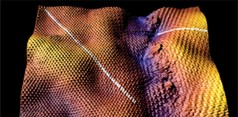 |
| Image of a grain boundary border |
Abstract:
Using graphene - either as an alternative to, or most likely as a complementary material with - silicon, offers the promise of much faster future electronics, along with several other advantages over the commonly used semiconductor. However, creating the one-atom thick sheets of carbon known as graphene in a way that could be easily integrated into mass production methods has proven difficult.
New research gives insight into graphene grain boundaries
Urbana, IL | Posted on January 15th, 2013When graphene is grown, lattices of the carbon grains are formed randomly, linked together at different angles of orientation in a hexagonal network. However, when those orientations become misaligned during the growth process, defects called grain boundaries (GBs) form. These boundaries scatter the flow of electrons in graphene, a fact that is detrimental to its successful electronic performance.
Beckman Institute researchers Joe Lyding and Eric Pop and their research groups have now given new insight into the electronics behavior of graphene with grain boundaries that could guide fabrication methods toward lessening their effect. The researchers grew polycrystalline graphene by chemical vapor deposition (CVD), using scanning tunneling microscopy and spectroscopy for analysis, to examine at the atomic scale grain boundaries on a silicon wafer. They reported their results in the journal ACS Nano.
"We obtained information about electron scattering at the boundaries that shows it significantly limits the electronic performance compared to grain boundary free graphene," Lyding said. "Grain boundaries form during graphene growth by CVD, and, while there is much worldwide effort to minimize the occurrence of grain boundaries, they are a fact of life for now.
"For electronics you would want to be able to make it on a wafer scale. Boundary free graphene is a key goal. In the interim we have to live with the grain boundaries, so understanding them is what we're trying to do."
Lyding compared graphene lattices made with the CVD method to pieces of a cyclone fence.
"If you had two pieces of fence, and you laid them on the ground next to each other but they weren't perfectly aligned, then they wouldn't match," he said. "That's a grain boundary, where the lattice doesn't match."
The research involved Pop's group, led by Beckman Fellow Josh Wood, growing the graphene at the Micro and Nanotechnology Lab, and transferring the thin films to a silicon (Si02) wafer. They then used the STM at Beckman developed by Lyding for analysis, led by first author Justin Koepke of Lyding's group.
Their analysis showed that when the electrons' itinerary takes them to a grain boundary, it is like, Lyding said, hitting a hill.
"The electrons hit this hill, they bounce off, they interfere with themselves and you actually see a standing wave pattern," he said. "It's a barrier so they have to go up and over that hill. Like anything else, that is going to slow them down. That's what Justin was able to measure with these spectroscopy measurements.
"Basically a grain boundary is a resistor in series with a conductor. That's always bad. It means it's going to take longer for an electron to get from point A to point B with some voltage applied."
Images from the STM reveal grain boundaries that suggest two pieces of cloth sewn together, Lyding said, by "a really bad tailor."
In the paper, the researchers were able to report on their analysis of the orientation angles between pieces of graphene as they grew together, and found "no preferential orientation angle between grains, and the GBs are continuous across graphene wrinkles and Si02 topography." They reported that analysis of those patterns "indicates that backscattering and intervalley scattering are the dominant mechanisms responsible for the mobility reduction in the presence of GBs in CVD-grown graphene."
Lyding said that the relationship between the orientation angle of the pieces of graphene and the wavelength of an electron impinges on the electron's movement at the grain boundary, leading to variations in their scattering.
"More scattering means that it is making it more difficult for an electron to move from one grain to the next," he said. "The more difficult you make that, the lower the quality of the electronic performance of any device made from that graphene."
The researchers work is aimed not just at understanding, but also at controlling grain boundaries. One of their findings - that GBs are aperiodic - replicated other work and could have implications for controlling them, as they wrote in the paper: "Combining the spectroscopic and scattering results suggest that GBs that are more periodic and well-ordered lead to reduced scattering from the GBs."
"I think if you have to live with grain boundaries you would like to be able to control exactly what their orientation is and choose an angle that minimizes the scattering," Lyding said.
By Steve McGaughey
####
About Beckman Institute for Advanced Science and Technology
The Institute's primary mission is to foster interdisciplinary work of the highest quality, transcending many of the limitations inherent in traditional university organizations and structures. The Institute was founded on the premise that reducing the barriers between traditional scientific and technological disciplines can yield research advances that more conventional approaches cannot.
For more information, please click here
Contacts:
Steve McGaughey
217-244-5582
Copyright © Beckman Institute for Advanced Science and Technology
If you have a comment, please Contact us.Issuers of news releases, not 7th Wave, Inc. or Nanotechnology Now, are solely responsible for the accuracy of the content.
Bookmark:


| Related News Press |
News and information
![]() Quantum computer improves AI predictions April 17th, 2026
Quantum computer improves AI predictions April 17th, 2026
![]() Flexible sensor gains sensitivity under pressure April 17th, 2026
Flexible sensor gains sensitivity under pressure April 17th, 2026
![]() A reusable chip for particulate matter sensing April 17th, 2026
A reusable chip for particulate matter sensing April 17th, 2026
![]() Detecting vibrational quantum beating in the predissociation dynamics of SF6 using time-resolved photoelectron spectroscopy April 17th, 2026
Detecting vibrational quantum beating in the predissociation dynamics of SF6 using time-resolved photoelectron spectroscopy April 17th, 2026
Thin films
![]() Tiny nanosheets, big leap: A new sensor detects ethanol at ultra-low levels January 30th, 2026
Tiny nanosheets, big leap: A new sensor detects ethanol at ultra-low levels January 30th, 2026
Graphene/ Graphite
![]() Electrifying results shed light on graphene foam as a potential material for lab grown cartilage June 6th, 2025
Electrifying results shed light on graphene foam as a potential material for lab grown cartilage June 6th, 2025
![]() Breakthrough in proton barrier films using pore-free graphene oxide: Kumamoto University researchers achieve new milestone in advanced coating technologies September 13th, 2024
Breakthrough in proton barrier films using pore-free graphene oxide: Kumamoto University researchers achieve new milestone in advanced coating technologies September 13th, 2024
Chip Technology
![]() A reusable chip for particulate matter sensing April 17th, 2026
A reusable chip for particulate matter sensing April 17th, 2026
![]() Metasurfaces smooth light to boost magnetic sensing precision January 30th, 2026
Metasurfaces smooth light to boost magnetic sensing precision January 30th, 2026
Discoveries
![]() Quantum computer improves AI predictions April 17th, 2026
Quantum computer improves AI predictions April 17th, 2026
![]() Flexible sensor gains sensitivity under pressure April 17th, 2026
Flexible sensor gains sensitivity under pressure April 17th, 2026
![]() A reusable chip for particulate matter sensing April 17th, 2026
A reusable chip for particulate matter sensing April 17th, 2026
![]() Detecting vibrational quantum beating in the predissociation dynamics of SF6 using time-resolved photoelectron spectroscopy April 17th, 2026
Detecting vibrational quantum beating in the predissociation dynamics of SF6 using time-resolved photoelectron spectroscopy April 17th, 2026
Announcements
![]() A fundamentally new therapeutic approach to cystic fibrosis: Nanobody repairs cellular defect April 17th, 2026
A fundamentally new therapeutic approach to cystic fibrosis: Nanobody repairs cellular defect April 17th, 2026
![]() UC Irvine physicists discover method to reverse �quantum scrambling� : The work addresses the problem of information loss in quantum computing system April 17th, 2026
UC Irvine physicists discover method to reverse �quantum scrambling� : The work addresses the problem of information loss in quantum computing system April 17th, 2026
|
|
||
|
|
||
| The latest news from around the world, FREE | ||
|
|
||
|
|
||
| Premium Products | ||
|
|
||
|
Only the news you want to read!
Learn More |
||
|
|
||
|
Full-service, expert consulting
Learn More |
||
|
|
||