Home > Press > Low-resistance connections facilitate multi-walled carbon nanotubes for interconnects: Hybrid electronics
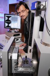 |
| Georgia Tech Professor Andrei Fedorov demonstrates the electron beam induced deposition (EBID) system used to create graphitic nanojoints to multi-walled carbon nanotubes.
Credit: Georgia Tech Photo: Gary Meek |
Abstract:
Using a new method for precisely controlling the deposition of carbon, researchers have demonstrated a technique for connecting multi-walled carbon nanotubes to the metallic pads of integrated circuits without the high interface resistance produced by traditional fabrication techniques.
Low-resistance connections facilitate multi-walled carbon nanotubes for interconnects: Hybrid electronics
Atlanta, GA | Posted on October 30th, 2012Based on electron beam-induced deposition (EBID), the work is believed to be the first to connect multiple shells of a multi-walled carbon nanotube to metal terminals on a semiconducting substrate, which is relevant to integrated circuit fabrication. Using this three-dimensional fabrication technique, researchers at the Georgia Institute of Technology developed graphitic nanojoints on both ends of the multi-walled carbon nanotubes, which yielded a 10-fold decrease in resistivity in its connection to metal junctions.
The technique could facilitate the integration of carbon nanotubes as interconnects in next-generation integrated circuits that use both silicon and carbon components. The research was supported by the Semiconductor Research Corporation, and in its early stages, by the National Science Foundation. The work was reported online October 4, 2012, by the journal IEEE Transactions on Nanotechnology.
"For the first time, we have established connections to multiple shells of carbon nanotubes with a technique that is amenable to integration with conventional integrated circuit microfabrication processes," said Andrei Fedorov, a professor in the George W. Woodruff School of Mechanical Engineering at Georgia Tech. "Connecting to multiple shells allows us to dramatically reduce the resistance and move to the next level of device performance."
In developing the new technique, the researchers relied on modeling to guide their process parameters. To make it scalable for manufacturing, they also worked toward technologies for isolating and aligning individual carbon nanotubes between the metal terminals on a silicon substrate, and for examining the properties of the resulting structures. The researchers believe the technique could also be used to connect multi-layered graphene to metal contacts, though their published research has so far focused on carbon nanotubes.
The low-temperature EBID process takes place in a scanning electron microscope (SEM) system modified for material deposition. The SEM's vacuum chamber is altered to introduce precursors of the materials that researchers would like to deposit. The electron gun normally used for imaging of nanostructures is instead used to generate low energy secondary electrons when the high energy primary electrons impinge on the substrate at carefully chosen locations. When the secondary electrons interact with hydrocarbon precursor molecules introduced into the SEM chamber, carbon is deposited in desired locations.
Unique to the EBID process, the deposited carbon makes a strong, chemically-bonded connection to the ends of the carbon nanotubes, unlike the weakly-coupled physical interface made in traditional techniques based on metal evaporation. Prior to deposition, the ends of the nanotubes are opened using an etching process, so the deposited carbon grows into the open end of the nanotube to electronically connect multiple shells. Thermal annealing of the carbon after deposition converts it to a crystalline graphitic form that significantly improves electrical conductivity.
"Atom-by-atom, we can build the connection where the electron beam strikes right near the open end of the carbon nanotubes," Fedorov explained. "The highest rate of deposition occurs where the concentration of precursor is high and there are a lot of secondary electrons. This provides a nanoscale sculpturing tool with three-dimensional control for connecting the open ends of carbon nanotubes on any desired substrate."
Multi-walled carbon nanotubes offer the promise of higher information delivery throughput for certain interconnects used in electronic devices. Researchers have envisioned a future generation of hybrid devices based on traditional integrated circuits but using interconnects based on carbon nanotubes.
Until now, however, resistance at the connections between the carbon structures and conventional silicon electronics has been too high to make the devices practical.
"The big challenge in this field is to make a connection not just to a single shell of a carbon nanotube," said Fedorov. "If only the outer wall of a carbon nanotube is connected, you really don't gain much because most of the transmission channel is under-utilized or not utilized at all."
The technique developed by Fedorov and his collaborators produces record low resistivity at the connection between the carbon nanotube and the metal pad. The researchers have measured resistance as low as approximately 100 Ohms - a factor of ten lower than the best that had been measured with other connection techniques.
"This technique gives us many new opportunities to go forward with integrating these carbon nanostructures into conventional devices," he said. "Because it is carbon, this interface has an advantage because its properties are similar to those of the carbon nanotubes to which they are providing a connection."
The researchers don't know exactly how many of the carbon nanotube shells are connected, but based on resistance measurements, they believe at least 10 of the approximately 30 conducting shells are contributing to electrical conduction.
However, handling carbon nanotubes poses a significant challenge to their use as interconnects. When formed through the electric arc technique, for example, carbon nanotubes are produced as a tangle of structures with varying lengths and properties, some with mechanical defects. Techniques have been developed to separate out single nanotubes, and to open their ends.
Fedorov and his collaborators - current and former graduate students Songkil Kim, Dhaval Kulkarni, Konrad Rykaczewski and Mathias Henry, along with Georgia Tech professor Vladimir Tsukruk - developed a method for aligning the multi-walled nanotubes across electronic contacts using focused electrical fields in combination with a substrate template created through electron beam lithography. The process has a significantly improved yield of properly aligned carbon nanotubes, with a potential for scalability over a large chip area.
Once the nanotubes are placed into their positions, the carbon is deposited using the EBID process, followed by graphitization. The phase transformation in the carbon interface is monitored using Raman spectroscopy to ensure that the material is transformed into its optimal nanocrystalline graphite state.
"Only by making advances in each of these areas can we achieve this technological advance, which is an enabling technology for nanoelectronics based on carbon materials," he said. "This is really a critical step for making many different kinds of devices using carbon nanotubes or graphene."
Before the new technique can be used on a large scale, researchers will have to improve their technique for aligning carbon nanotubes and develop EBID systems able to deposit connectors on multiple devices simultaneously. Advances in parallel electron beam systems may provide a way to mass-produce the connections, Fedorov said.
"A major amount of work remains to be done in this area, but we believe this is possible if industry becomes interested," he noted. "There are applications where integrating carbon nanotubes into circuits could be very attractive."
CITATION: Songkil Kim, et.al, "Fabrication of an Ultra-Low-Resistance Ohmic Contact to MWCNT-Metal Interconnect Using Graphitic Carbon by Electron Beam Induced Deposition (EBID)", IEEE Transactions on Nanotechnology (2012). dx.doi.org/10.1109/TNANO.2012.2220377
This research has been supported by the Semiconductor Research Corporation (SRC) under GRC grant 2008OJ1864.1281 and in part by the National Science Foundation (NSF) under grant DMI 0403671. The content of this article is solely the responsibility of the authors and does not necessarily represent the official views of the NSF or the SRC.
####
For more information, please click here
Contacts:
John Toon
404-894-6986
Abby Vogel Robinson
404-385-3364
Copyright © Georgia Institute of Technology Research News
If you have a comment, please Contact us.Issuers of news releases, not 7th Wave, Inc. or Nanotechnology Now, are solely responsible for the accuracy of the content.
Bookmark:


| Related Links |
| Related News Press |
News and information
![]() Quantum computer improves AI predictions April 17th, 2026
Quantum computer improves AI predictions April 17th, 2026
![]() Flexible sensor gains sensitivity under pressure April 17th, 2026
Flexible sensor gains sensitivity under pressure April 17th, 2026
![]() A reusable chip for particulate matter sensing April 17th, 2026
A reusable chip for particulate matter sensing April 17th, 2026
![]() Detecting vibrational quantum beating in the predissociation dynamics of SF6 using time-resolved photoelectron spectroscopy April 17th, 2026
Detecting vibrational quantum beating in the predissociation dynamics of SF6 using time-resolved photoelectron spectroscopy April 17th, 2026
Chip Technology
![]() A reusable chip for particulate matter sensing April 17th, 2026
A reusable chip for particulate matter sensing April 17th, 2026
![]() Metasurfaces smooth light to boost magnetic sensing precision January 30th, 2026
Metasurfaces smooth light to boost magnetic sensing precision January 30th, 2026
Nanotubes/Buckyballs/Fullerenes/Nanorods/Nanostrings/Nanosheets
![]() Tiny nanosheets, big leap: A new sensor detects ethanol at ultra-low levels January 30th, 2026
Tiny nanosheets, big leap: A new sensor detects ethanol at ultra-low levels January 30th, 2026
![]() Enhancing power factor of p- and n-type single-walled carbon nanotubes April 25th, 2025
Enhancing power factor of p- and n-type single-walled carbon nanotubes April 25th, 2025
![]() Chainmail-like material could be the future of armor: First 2D mechanically interlocked polymer exhibits exceptional flexibility and strength January 17th, 2025
Chainmail-like material could be the future of armor: First 2D mechanically interlocked polymer exhibits exceptional flexibility and strength January 17th, 2025
![]() Innovative biomimetic superhydrophobic coating combines repair and buffering properties for superior anti-erosion December 13th, 2024
Innovative biomimetic superhydrophobic coating combines repair and buffering properties for superior anti-erosion December 13th, 2024
Discoveries
![]() Quantum computer improves AI predictions April 17th, 2026
Quantum computer improves AI predictions April 17th, 2026
![]() Flexible sensor gains sensitivity under pressure April 17th, 2026
Flexible sensor gains sensitivity under pressure April 17th, 2026
![]() A reusable chip for particulate matter sensing April 17th, 2026
A reusable chip for particulate matter sensing April 17th, 2026
![]() Detecting vibrational quantum beating in the predissociation dynamics of SF6 using time-resolved photoelectron spectroscopy April 17th, 2026
Detecting vibrational quantum beating in the predissociation dynamics of SF6 using time-resolved photoelectron spectroscopy April 17th, 2026
Announcements
![]() A fundamentally new therapeutic approach to cystic fibrosis: Nanobody repairs cellular defect April 17th, 2026
A fundamentally new therapeutic approach to cystic fibrosis: Nanobody repairs cellular defect April 17th, 2026
![]() UC Irvine physicists discover method to reverse �quantum scrambling� : The work addresses the problem of information loss in quantum computing system April 17th, 2026
UC Irvine physicists discover method to reverse �quantum scrambling� : The work addresses the problem of information loss in quantum computing system April 17th, 2026
Tools
![]() Metasurfaces smooth light to boost magnetic sensing precision January 30th, 2026
Metasurfaces smooth light to boost magnetic sensing precision January 30th, 2026
![]() From sensors to smart systems: the rise of AI-driven photonic noses January 30th, 2026
From sensors to smart systems: the rise of AI-driven photonic noses January 30th, 2026
![]() Japan launches fully domestically produced quantum computer: Expo visitors to experience quantum computing firsthand August 8th, 2025
Japan launches fully domestically produced quantum computer: Expo visitors to experience quantum computing firsthand August 8th, 2025
|
|
||
|
|
||
| The latest news from around the world, FREE | ||
|
|
||
|
|
||
| Premium Products | ||
|
|
||
|
Only the news you want to read!
Learn More |
||
|
|
||
|
Full-service, expert consulting
Learn More |
||
|
|
||