Home > Press > NRL Demonstrates High Durability of Nanotube Transistors to the Harsh Space Environment
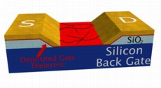 |
| A locally etched back-gated field effect transistor (FET) structure with a deposited dielectric layer. Thick dielectric layers are highly susceptible to radiation induced charge build-up, which is known to cause threshold voltage shifts and increased leakage in metal-oxide semiconductor (MOS) devices. To mitigate these effects, the dielectric layer is locally etched in the active region of the back-gated FET. A gate dielectric material is then deposited (depicted in red) over the entire substrate. (Photo: U.S. Naval Research Laboratory) |
Abstract:
U.S. Naval Research Laboratory electronics science and technology engineers demonstrate the ability of single walled carbon nanotube transistors (SWCNTs) to survive the harsh space environment, investigating the effects of ionizing radiation on the crystalline structures and further supporting the development of SWCNT-based nanoelectronics for use in harsh radiation environments.
NRL Demonstrates High Durability of Nanotube Transistors to the Harsh Space Environment
Washington, DC | Posted on September 21st, 2012"One of the primary challenges for space electronics is mitigating the susceptibility of prolonged exposure to radiation that exists in the charged particle belts that encircle Earth," said Cory Cress, materials research engineer. "These are the first controlled demonstrations showing little performance degradation and high tolerance to cumulative ionizing radiation exposure."
Radiation effects take two forms, transient effects and cumulative effects. The former, referred to as single effect transients (SETs), result from a direct strike by an ionizing particle in space that causes a current pulse in the device. If this pulse propagates through the circuit it can cause data corruption that can be extremely detrimental to someone that relies on that signal, such as a person using GPS for navigation. NRL researchers have recently predicted that such effects are nearly eliminated for SWCNT-based nanoelectronics due to their small size, low density, and inherent isolation from neighboring SWCNTs in a device.
The cumulative effects in traditional electronics results from trapped charges in the oxides of the devices, including the gate oxide and those used to isolate adjacent devices, the latter being primary source of radiation-induced performance degradation in state-of-the-art complementary metal-oxide semiconductor (CMOS) devices. The effect is manifested as a shift in the voltage needed to turn the transistor on or off. This initially results in power leakage, but can eventually cause failure of the entire circuit.
By developing a SWCNT structure with a thin gate oxide made from thin silicon oxynitride, NRL researchers recently demonstrated SWCNT transistors that do not suffer from such radiation-induced performance changes. This hardened dielectric material and naturally isolated one-dimensional SWCNT structure makes them extremely radiation tolerant.
The ability for SWCNT-based transistors to be both tolerant to transient and cumulative effects potentially enables future space electronics with less redundancy and error-correction circuitry, while maintaining the same quality of fidelity. This reduction in overhead alone would greatly reduce power and improve performance over existing space-electronic systems even if the SWCNT-based transistors operate at the same speed as current technologies. Even greater benefits are foreseeable in the future, once devices are developed that exceed the performance of silicon-based transistors.
####
About U.S. Naval Research Laboratory
The U.S. Naval Research Laboratory is the Navy's full-spectrum corporate laboratory, conducting a broadly based multidisciplinary program of scientific research and advanced technological development. The Laboratory, with a total complement of nearly 2,500 personnel, is located in southwest Washington, D.C., with other major sites at the Stennis Space Center, Miss., and Monterey, Calif. NRL has served the Navy and the nation for over 85 years and continues to meet the complex technological challenges of today's world. For more information, visit the NRL homepage or join the conversation on Twitter, Facebook, and YouTube.
For more information, please click here
Contacts:
U.S. Naval Research Laboratory
Daniel Parry, 202-767-2541
Copyright © U.S. Naval Research Laboratory
If you have a comment, please Contact us.Issuers of news releases, not 7th Wave, Inc. or Nanotechnology Now, are solely responsible for the accuracy of the content.
Bookmark:


| Related News Press |
News and information
![]() Quantum computer improves AI predictions April 17th, 2026
Quantum computer improves AI predictions April 17th, 2026
![]() Flexible sensor gains sensitivity under pressure April 17th, 2026
Flexible sensor gains sensitivity under pressure April 17th, 2026
![]() A reusable chip for particulate matter sensing April 17th, 2026
A reusable chip for particulate matter sensing April 17th, 2026
![]() Detecting vibrational quantum beating in the predissociation dynamics of SF6 using time-resolved photoelectron spectroscopy April 17th, 2026
Detecting vibrational quantum beating in the predissociation dynamics of SF6 using time-resolved photoelectron spectroscopy April 17th, 2026
Laboratories
![]() Researchers develop molecular qubits that communicate at telecom frequencies October 3rd, 2025
Researchers develop molecular qubits that communicate at telecom frequencies October 3rd, 2025
![]() A battery�s hopping ions remember where they�ve been: Seen in atomic detail, the seemingly smooth flow of ions through a battery�s electrolyte is surprisingly complicated February 16th, 2024
A battery�s hopping ions remember where they�ve been: Seen in atomic detail, the seemingly smooth flow of ions through a battery�s electrolyte is surprisingly complicated February 16th, 2024
Govt.-Legislation/Regulation/Funding/Policy
![]() Quantum computer improves AI predictions April 17th, 2026
Quantum computer improves AI predictions April 17th, 2026
![]() Metasurfaces smooth light to boost magnetic sensing precision January 30th, 2026
Metasurfaces smooth light to boost magnetic sensing precision January 30th, 2026
![]() New imaging approach transforms study of bacterial biofilms August 8th, 2025
New imaging approach transforms study of bacterial biofilms August 8th, 2025
Chip Technology
![]() A reusable chip for particulate matter sensing April 17th, 2026
A reusable chip for particulate matter sensing April 17th, 2026
![]() Metasurfaces smooth light to boost magnetic sensing precision January 30th, 2026
Metasurfaces smooth light to boost magnetic sensing precision January 30th, 2026
Nanotubes/Buckyballs/Fullerenes/Nanorods/Nanostrings/Nanosheets
![]() Tiny nanosheets, big leap: A new sensor detects ethanol at ultra-low levels January 30th, 2026
Tiny nanosheets, big leap: A new sensor detects ethanol at ultra-low levels January 30th, 2026
![]() Enhancing power factor of p- and n-type single-walled carbon nanotubes April 25th, 2025
Enhancing power factor of p- and n-type single-walled carbon nanotubes April 25th, 2025
![]() Chainmail-like material could be the future of armor: First 2D mechanically interlocked polymer exhibits exceptional flexibility and strength January 17th, 2025
Chainmail-like material could be the future of armor: First 2D mechanically interlocked polymer exhibits exceptional flexibility and strength January 17th, 2025
![]() Innovative biomimetic superhydrophobic coating combines repair and buffering properties for superior anti-erosion December 13th, 2024
Innovative biomimetic superhydrophobic coating combines repair and buffering properties for superior anti-erosion December 13th, 2024
Announcements
![]() A fundamentally new therapeutic approach to cystic fibrosis: Nanobody repairs cellular defect April 17th, 2026
A fundamentally new therapeutic approach to cystic fibrosis: Nanobody repairs cellular defect April 17th, 2026
![]() UC Irvine physicists discover method to reverse �quantum scrambling� : The work addresses the problem of information loss in quantum computing system April 17th, 2026
UC Irvine physicists discover method to reverse �quantum scrambling� : The work addresses the problem of information loss in quantum computing system April 17th, 2026
Military
![]() Quantum engineers �squeeze� laser frequency combs to make more sensitive gas sensors January 17th, 2025
Quantum engineers �squeeze� laser frequency combs to make more sensitive gas sensors January 17th, 2025
![]() Chainmail-like material could be the future of armor: First 2D mechanically interlocked polymer exhibits exceptional flexibility and strength January 17th, 2025
Chainmail-like material could be the future of armor: First 2D mechanically interlocked polymer exhibits exceptional flexibility and strength January 17th, 2025
![]() Single atoms show their true color July 5th, 2024
Single atoms show their true color July 5th, 2024
![]() NRL charters Navy�s quantum inertial navigation path to reduce drift April 5th, 2024
NRL charters Navy�s quantum inertial navigation path to reduce drift April 5th, 2024
Aerospace/Space
![]() Decoding hydrogen‑bond network of electrolyte for cryogenic durable aqueous zinc‑ion batteries January 30th, 2026
Decoding hydrogen‑bond network of electrolyte for cryogenic durable aqueous zinc‑ion batteries January 30th, 2026
![]() ICFO researchers overcome long-standing bottleneck in single photon detection with twisted 2D materials August 8th, 2025
ICFO researchers overcome long-standing bottleneck in single photon detection with twisted 2D materials August 8th, 2025
![]() Onion-like nanoparticles found in aircraft exhaust May 14th, 2025
Onion-like nanoparticles found in aircraft exhaust May 14th, 2025
|
|
||
|
|
||
| The latest news from around the world, FREE | ||
|
|
||
|
|
||
| Premium Products | ||
|
|
||
|
Only the news you want to read!
Learn More |
||
|
|
||
|
Full-service, expert consulting
Learn More |
||
|
|
||