Home > Press > Scientists researching graphene stumble upon surprising result
 |
Abstract:
Researchers from the United Kingdom have uncovered an unexpected characteristic of graphene by demonstrating a method that uses graphene as a building block to create new three-dimensional (3D) crystal structures which are not confined by what nature can produce.
Scientists researching graphene stumble upon surprising result
Manchester, UK | Posted on July 30th, 2012Set out in the journal Nature Materials, their method involves sandwiching individual graphene sheets between insulating layers in order to produce electrical devices with unique new properties.
The hope is that this new method will open up a whole new dimension of physics research.
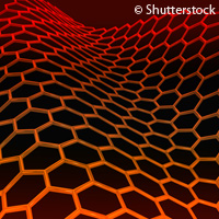
Graphene is a 2D material consisting of a single layer of carbon atoms arranged in a honeycomb or chicken wire structure. It is the thinnest material in the world and yet is also one of the strongest. It conducts electricity as efficiently as copper and outperforms all other materials as a conductor of heat.
The scientists proved that a new side-view imaging technique can be used to visualise the individual atomic layers of graphene within the devices they have built. They found that the structures were almost perfect even when more than 10 different layers were used to build the stack.
This development further proves graphene's suitability as a major component in the next generation of computer chips.
The researchers' side-view imaging approach works by first extracting a thin slice from the centre of the device. The team likens this to cutting through a rock to reveal the geological layers or slicing into a chocolate cake to reveal the individual layers of icing.
The scientists used a beam of ions to cut into the surface of the graphene and dig a trench on either side of the section they wanted to isolate. They then removed a thin slice of the device.
Lead study author Dr Sarah Haigh, from the University of Manchester, comments: 'Our slices are only around 100 atoms thick and this allows us to visualise the individual atomic layers of graphene in projection.
'We have found that the observed roughness of the graphene is correlated with their conductivity. Of course we have to make all our electrical measurements before cutting into the device. We were also able to observe that the layers were perfectly clean and that any debris left over from production segregated into isolated pockets and so did not affect device performance. We plan to use this new side view imaging approach to improve the performance of our graphene devices.'
Two of the study researchers, Andre Geim and Konstantin Novoselov, both from the University of Manchester, were awarded the Nobel Prize in Physics in 2010 for their 'groundbreaking experiments regarding the two-dimensional material graphene'.
####
For more information, please click here
Copyright © Cordis
If you have a comment, please Contact us.Issuers of news releases, not 7th Wave, Inc. or Nanotechnology Now, are solely responsible for the accuracy of the content.
Bookmark:


| Related News Press |
News and information
![]() Quantum computer improves AI predictions April 17th, 2026
Quantum computer improves AI predictions April 17th, 2026
![]() Flexible sensor gains sensitivity under pressure April 17th, 2026
Flexible sensor gains sensitivity under pressure April 17th, 2026
![]() A reusable chip for particulate matter sensing April 17th, 2026
A reusable chip for particulate matter sensing April 17th, 2026
![]() Detecting vibrational quantum beating in the predissociation dynamics of SF6 using time-resolved photoelectron spectroscopy April 17th, 2026
Detecting vibrational quantum beating in the predissociation dynamics of SF6 using time-resolved photoelectron spectroscopy April 17th, 2026
Imaging
![]() Simple algorithm paired with standard imaging tool could predict failure in lithium metal batteries August 8th, 2025
Simple algorithm paired with standard imaging tool could predict failure in lithium metal batteries August 8th, 2025
Graphene/ Graphite
![]() Electrifying results shed light on graphene foam as a potential material for lab grown cartilage June 6th, 2025
Electrifying results shed light on graphene foam as a potential material for lab grown cartilage June 6th, 2025
![]() Breakthrough in proton barrier films using pore-free graphene oxide: Kumamoto University researchers achieve new milestone in advanced coating technologies September 13th, 2024
Breakthrough in proton barrier films using pore-free graphene oxide: Kumamoto University researchers achieve new milestone in advanced coating technologies September 13th, 2024
Chip Technology
![]() A reusable chip for particulate matter sensing April 17th, 2026
A reusable chip for particulate matter sensing April 17th, 2026
![]() Metasurfaces smooth light to boost magnetic sensing precision January 30th, 2026
Metasurfaces smooth light to boost magnetic sensing precision January 30th, 2026
Discoveries
![]() Quantum computer improves AI predictions April 17th, 2026
Quantum computer improves AI predictions April 17th, 2026
![]() Flexible sensor gains sensitivity under pressure April 17th, 2026
Flexible sensor gains sensitivity under pressure April 17th, 2026
![]() A reusable chip for particulate matter sensing April 17th, 2026
A reusable chip for particulate matter sensing April 17th, 2026
![]() Detecting vibrational quantum beating in the predissociation dynamics of SF6 using time-resolved photoelectron spectroscopy April 17th, 2026
Detecting vibrational quantum beating in the predissociation dynamics of SF6 using time-resolved photoelectron spectroscopy April 17th, 2026
Announcements
![]() A fundamentally new therapeutic approach to cystic fibrosis: Nanobody repairs cellular defect April 17th, 2026
A fundamentally new therapeutic approach to cystic fibrosis: Nanobody repairs cellular defect April 17th, 2026
![]() UC Irvine physicists discover method to reverse �quantum scrambling� : The work addresses the problem of information loss in quantum computing system April 17th, 2026
UC Irvine physicists discover method to reverse �quantum scrambling� : The work addresses the problem of information loss in quantum computing system April 17th, 2026
Grants/Sponsored Research/Awards/Scholarships/Gifts/Contests/Honors/Records
![]() Quantum computer improves AI predictions April 17th, 2026
Quantum computer improves AI predictions April 17th, 2026
![]() Detecting vibrational quantum beating in the predissociation dynamics of SF6 using time-resolved photoelectron spectroscopy April 17th, 2026
Detecting vibrational quantum beating in the predissociation dynamics of SF6 using time-resolved photoelectron spectroscopy April 17th, 2026
![]() Metasurfaces smooth light to boost magnetic sensing precision January 30th, 2026
Metasurfaces smooth light to boost magnetic sensing precision January 30th, 2026
|
|
||
|
|
||
| The latest news from around the world, FREE | ||
|
|
||
|
|
||
| Premium Products | ||
|
|
||
|
Only the news you want to read!
Learn More |
||
|
|
||
|
Full-service, expert consulting
Learn More |
||
|
|
||