Home > Press > Solar nanowire array may increase percentage of sun's frequencies available for energy conversion: Sandia nanowire template permits flexible energy absorption
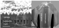 |
| Cross-sectional images of the indium gallium nitride nanowire solar cell. (Image courtesy of Sandia National Laboratories) |
Abstract:
Researchers creating electricity through photovoltaics want to convert as many of the sun's wavelengths as possible to achieve maximum efficiency. Otherwise, they're eating only a small part of a shot duck: wasting time and money by using only a tiny bit of the sun's incoming energies.
Solar nanowire array may increase percentage of sun's frequencies available for energy conversion: Sandia nanowire template permits flexible energy absorption
Albuquerque, NM | Posted on June 20th, 2012For this reason, they see indium gallium nitride as a valuable future material for photovoltaic systems. Changing the concentration of indium allows researchers to tune the material's response so it collects solar energy from a variety of wavelengths. The more variations designed into the system, the more of the solar spectrum can be absorbed, leading to increased solar cell efficiencies. Silicon, today's photovoltaic industry standard, is limited in the wavelength range it can 'see' and absorb.
But there is a problem: Indium gallium nitride, part of a family of materials called III-nitrides, is typically grown on thin films of gallium nitride. Because gallium nitride atomic layers have different crystal lattice spacings from indium gallium nitride atomic layers, the mismatch leads to structural strain that limits both the layer thickness and percentage of indium that can be added. Thus, increasing the percentage of indium added broadens the solar spectrum that can be collected, but reduces the material's ability to tolerate the strain.
Cross-sectional images of the indium gallium nitride nanowire solar cell. (Image courtesy of Sandia National Laboratories) Click on thumbnail for a high-resolution image.
Sandia National Laboratories scientists Jonathan Wierer Jr. and George Wang reported in the journal Nanotechnology that if the indium mixture is grown on a phalanx of nanowires rather than on a flat surface, the small surface areas of the nanowires allow the indium shell layer to partially "relax" along each wire, easing strain. This relaxation allowed the team to create a nanowire solar cell with indium percentages of roughly 33 percent, higher than any other reported attempt at creating III-nitride solar cells.
This initial attempt also lowered the absorption base energy from 2.4eV to 2.1 eV, the lowest of any III-nitride solar cell to date, and made a wider range of wavelengths available for power conversion. Power conversion efficiencies were low � only 0.3 percent compared to a standard commercial cell that hums along at about 15 percent � but the demonstration took place on imperfect nanowire-array templates. Refinements should lead to higher efficiencies and even lower energies.
Several unique techniques were used to create the III-nitride nanowire array solar cell. A top-down fabrication process was used to create the nanowire array by masking a gallium nitride (GaN) layer with a colloidal silica mask, followed by dry and wet etching. The resulting array consisted of nanowires with vertical sidewalls and of uniform height.
Next, shell layers containing the higher indium percentage of indium gallium nitride (InGaN) were formed on the GaN nanowire template via metal organic chemical vapor deposition. Lastly, In0.02Ga0.98N was grown, in such a way that caused the nanowires to coalescence. This process produced a canopy layer at the top, facilitating simple planar processing and making the technology manufacturable.
The results, says Wierer, although modest, represent a promising path forward for III-nitride solar cell research. The nano-architecture not only enables higher indium proportion in the InGaN layers but also increased absorption via light scattering in the faceted InGaN canopy layer, as well as air voids that guide light within the nanowire array.
The research was funded by DOE's Office of Science through the Solid State Lighting Science Energy Frontier Research Center, and Sandia's Laboratory Directed Research and Development program.
####
About DOE/Sandia National Laboratories
Sandia National Laboratories is a multi-program laboratory operated by Sandia Corporation, a wholly owned subsidiary of Lockheed Martin company, for the U.S. Department of Energy's National Nuclear Security Administration. With main facilities in Albuquerque, N.M., and Livermore, Calif., Sandia has major R&D responsibilities in national security, energy and environmental technologies and economic competitiveness.
For more information, please click here
Contacts:
Neal Singer
505-845-7078
Copyright © DOE/Sandia National Laboratories
If you have a comment, please Contact us.Issuers of news releases, not 7th Wave, Inc. or Nanotechnology Now, are solely responsible for the accuracy of the content.
Bookmark:


| Related News Press |
News and information
![]() Quantum computer improves AI predictions April 17th, 2026
Quantum computer improves AI predictions April 17th, 2026
![]() Flexible sensor gains sensitivity under pressure April 17th, 2026
Flexible sensor gains sensitivity under pressure April 17th, 2026
![]() A reusable chip for particulate matter sensing April 17th, 2026
A reusable chip for particulate matter sensing April 17th, 2026
![]() Detecting vibrational quantum beating in the predissociation dynamics of SF6 using time-resolved photoelectron spectroscopy April 17th, 2026
Detecting vibrational quantum beating in the predissociation dynamics of SF6 using time-resolved photoelectron spectroscopy April 17th, 2026
Laboratories
![]() Researchers develop molecular qubits that communicate at telecom frequencies October 3rd, 2025
Researchers develop molecular qubits that communicate at telecom frequencies October 3rd, 2025
![]() A battery�s hopping ions remember where they�ve been: Seen in atomic detail, the seemingly smooth flow of ions through a battery�s electrolyte is surprisingly complicated February 16th, 2024
A battery�s hopping ions remember where they�ve been: Seen in atomic detail, the seemingly smooth flow of ions through a battery�s electrolyte is surprisingly complicated February 16th, 2024
Govt.-Legislation/Regulation/Funding/Policy
![]() Quantum computer improves AI predictions April 17th, 2026
Quantum computer improves AI predictions April 17th, 2026
![]() Metasurfaces smooth light to boost magnetic sensing precision January 30th, 2026
Metasurfaces smooth light to boost magnetic sensing precision January 30th, 2026
![]() New imaging approach transforms study of bacterial biofilms August 8th, 2025
New imaging approach transforms study of bacterial biofilms August 8th, 2025
Discoveries
![]() Quantum computer improves AI predictions April 17th, 2026
Quantum computer improves AI predictions April 17th, 2026
![]() Flexible sensor gains sensitivity under pressure April 17th, 2026
Flexible sensor gains sensitivity under pressure April 17th, 2026
![]() A reusable chip for particulate matter sensing April 17th, 2026
A reusable chip for particulate matter sensing April 17th, 2026
![]() Detecting vibrational quantum beating in the predissociation dynamics of SF6 using time-resolved photoelectron spectroscopy April 17th, 2026
Detecting vibrational quantum beating in the predissociation dynamics of SF6 using time-resolved photoelectron spectroscopy April 17th, 2026
Announcements
![]() A fundamentally new therapeutic approach to cystic fibrosis: Nanobody repairs cellular defect April 17th, 2026
A fundamentally new therapeutic approach to cystic fibrosis: Nanobody repairs cellular defect April 17th, 2026
![]() UC Irvine physicists discover method to reverse �quantum scrambling� : The work addresses the problem of information loss in quantum computing system April 17th, 2026
UC Irvine physicists discover method to reverse �quantum scrambling� : The work addresses the problem of information loss in quantum computing system April 17th, 2026
Energy
![]() Sensors innovations for smart lithium-based batteries: advancements, opportunities, and potential challenges August 8th, 2025
Sensors innovations for smart lithium-based batteries: advancements, opportunities, and potential challenges August 8th, 2025
![]() Simple algorithm paired with standard imaging tool could predict failure in lithium metal batteries August 8th, 2025
Simple algorithm paired with standard imaging tool could predict failure in lithium metal batteries August 8th, 2025
Solar/Photovoltaic
![]() Spinel-type sulfide semiconductors to operate the next-generation LEDs and solar cells For solar-cell absorbers and green-LED source October 3rd, 2025
Spinel-type sulfide semiconductors to operate the next-generation LEDs and solar cells For solar-cell absorbers and green-LED source October 3rd, 2025
![]() KAIST researchers introduce new and improved, next-generation perovskite solar cell November 8th, 2024
KAIST researchers introduce new and improved, next-generation perovskite solar cell November 8th, 2024
![]() Groundbreaking precision in single-molecule optoelectronics August 16th, 2024
Groundbreaking precision in single-molecule optoelectronics August 16th, 2024
![]() Development of zinc oxide nanopagoda array photoelectrode: photoelectrochemical water-splitting hydrogen production January 12th, 2024
Development of zinc oxide nanopagoda array photoelectrode: photoelectrochemical water-splitting hydrogen production January 12th, 2024
|
|
||
|
|
||
| The latest news from around the world, FREE | ||
|
|
||
|
|
||
| Premium Products | ||
|
|
||
|
Only the news you want to read!
Learn More |
||
|
|
||
|
Full-service, expert consulting
Learn More |
||
|
|
||