Home > Press > Carbon nanotubes best for 3D electronics
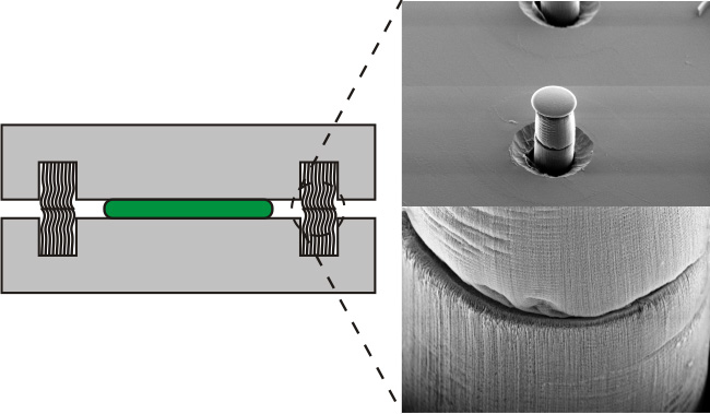 |
| Two chips have interconnects that are filled with thousands of carbon nanotubes. The chips are then bonded with adhesive so that the carbon nanotubes are directly contacted. A connection using two such interconnects is pictured to the right. Image credit: Teng Wang, Kjell Jeppson, Lilei Ye, Johan Liu. Carbon-Nanotube Through-Silicon Via Interconnects for Three-Dimensional Integration. Small, 2011, Volume 7, pages 2,313�2,317. Copyright Wiley-VCH Verlag GmbH & Co. KGaA. |
Abstract:
Researchers at Chalmers have demonstrated that two stacked chips can be vertically interconnected with carbon nanotube vias through the chips. This new method improves possibilities for 3D integration of circuits, one of the most promising approaches for miniaturization and performance promotion of electronics.
Carbon nanotubes best for 3D electronics
Gothenburg, Sweden | Posted on December 12th, 2011Three dimensional integration is a hot field within electronics since it offers a new way to package components densely and thus build tiny, well-functioning units. When stacking chips vertically, the most effective way to interconnect them is with electrical interconnects that go through the chip (instead of being wired together at the edges) - what are known as through-silicon vias.
The industry thus far has primarily used copper for this purpose; however, copper has several disadvantages that can limit the reliability of 3D electronics. Another major issue involves cooling when the chips get hot. The excellent thermal qualities of carbon nanotubes can play a decisive role in this respect.
Thus a research team at Chalmers is working with carbon nanotubes as conductive material for through-silicon vias. Carbon nanotubes - or tubes made of graphene whose walls are only one atom thick - are going to be the most reliable of all conductive materials if it is possible to use them on a large scale. This is the opinion of Kjell Jeppsson, a member of the research team.
"Potentially, carbon nanotubes have much better properties than copper, both in terms of thermal and electrical conductivity", he says. "Carbon nanotubes are also better suited for use with silicon from a purely mechanical point of view. They expand about the same amount as the surrounding silicon while copper expands more, which results in mechanical tension that can cause the components to break."
The researchers have demonstrated that two chips can be vertically interconnected with carbon nanotubes by through-silicon via interconnects, and that the chips can be bonded. They have also demonstrated that the same method can be used for electrical interconnection between the chip and the package.
PhD student Teng Wang - who defends his thesis on 12 December - has worked on production. He has developed a technique to fill through-silicon vias with thousands of carbon nanotubes. The chips are then bonded with an adhesive so that the carbon nanotubes are directly contacted and can thus conduct current through the chips.
"One difficulty involves producing carbon nanotubes with perfect properties and with the length we need to go through the chip," he says. "We have produced tubes that are 200 micrometers long, which can be compared to the diameter which is only 10 nanometers. Their properties, however, are not yet perfect."
For the method to be transferred to industrial production, manufacturing temperature needs to be reduced to a maximum of 450 degrees. This is a great challenge since carbon nanotubes are currently "grown" at a minimum of 700 degrees.
If successful, entirely new possibilities will arise for future shrinking of electronics - not least in terms of improved performance. The three dimensional integration using through-silicon vias provides significantly quicker signal transfers than traditional integration where chips are placed next to each other. Furthermore, through-silicon vias with carbon nanotubes provide less expensive production compared to the current technology that uses copper interconnects.
"There are several projects involving 3D integration underway in the industry, but there are potential problems with both cooling and reliability since they use copper," says Kjell Jeppsson. "If our method works on a large scale, I believe it will be in production within five years."
####
For more information, please click here
Contacts:
Kjell Jeppson
Department of Microtechnology and Nanoscience
+46 31-772 1856
Teng Wang
Department of Microtechnology and Nanoscience
+46 31-772 3092
Johan Liu
Department of Microtechnology and Nanoscience
+46 31-772 3067
Copyright © Chalmers University of Technology
If you have a comment, please Contact us.Issuers of news releases, not 7th Wave, Inc. or Nanotechnology Now, are solely responsible for the accuracy of the content.
Bookmark:


| Related Links |
![]() The PhD thesis that is defended on December 12:
The PhD thesis that is defended on December 12:
![]() Read the researchers' articles in the scientific journals Small and Advanced Materials:
Read the researchers' articles in the scientific journals Small and Advanced Materials:
| Related News Press |
News and information
![]() Quantum computer improves AI predictions April 17th, 2026
Quantum computer improves AI predictions April 17th, 2026
![]() Flexible sensor gains sensitivity under pressure April 17th, 2026
Flexible sensor gains sensitivity under pressure April 17th, 2026
![]() A reusable chip for particulate matter sensing April 17th, 2026
A reusable chip for particulate matter sensing April 17th, 2026
![]() Detecting vibrational quantum beating in the predissociation dynamics of SF6 using time-resolved photoelectron spectroscopy April 17th, 2026
Detecting vibrational quantum beating in the predissociation dynamics of SF6 using time-resolved photoelectron spectroscopy April 17th, 2026
Possible Futures
![]() A fundamentally new therapeutic approach to cystic fibrosis: Nanobody repairs cellular defect April 17th, 2026
A fundamentally new therapeutic approach to cystic fibrosis: Nanobody repairs cellular defect April 17th, 2026
![]() UC Irvine physicists discover method to reverse �quantum scrambling� : The work addresses the problem of information loss in quantum computing system April 17th, 2026
UC Irvine physicists discover method to reverse �quantum scrambling� : The work addresses the problem of information loss in quantum computing system April 17th, 2026
Chip Technology
![]() A reusable chip for particulate matter sensing April 17th, 2026
A reusable chip for particulate matter sensing April 17th, 2026
![]() Metasurfaces smooth light to boost magnetic sensing precision January 30th, 2026
Metasurfaces smooth light to boost magnetic sensing precision January 30th, 2026
Nanotubes/Buckyballs/Fullerenes/Nanorods/Nanostrings/Nanosheets
![]() Tiny nanosheets, big leap: A new sensor detects ethanol at ultra-low levels January 30th, 2026
Tiny nanosheets, big leap: A new sensor detects ethanol at ultra-low levels January 30th, 2026
![]() Enhancing power factor of p- and n-type single-walled carbon nanotubes April 25th, 2025
Enhancing power factor of p- and n-type single-walled carbon nanotubes April 25th, 2025
![]() Chainmail-like material could be the future of armor: First 2D mechanically interlocked polymer exhibits exceptional flexibility and strength January 17th, 2025
Chainmail-like material could be the future of armor: First 2D mechanically interlocked polymer exhibits exceptional flexibility and strength January 17th, 2025
![]() Innovative biomimetic superhydrophobic coating combines repair and buffering properties for superior anti-erosion December 13th, 2024
Innovative biomimetic superhydrophobic coating combines repair and buffering properties for superior anti-erosion December 13th, 2024
Discoveries
![]() Quantum computer improves AI predictions April 17th, 2026
Quantum computer improves AI predictions April 17th, 2026
![]() Flexible sensor gains sensitivity under pressure April 17th, 2026
Flexible sensor gains sensitivity under pressure April 17th, 2026
![]() A reusable chip for particulate matter sensing April 17th, 2026
A reusable chip for particulate matter sensing April 17th, 2026
![]() Detecting vibrational quantum beating in the predissociation dynamics of SF6 using time-resolved photoelectron spectroscopy April 17th, 2026
Detecting vibrational quantum beating in the predissociation dynamics of SF6 using time-resolved photoelectron spectroscopy April 17th, 2026
Announcements
![]() A fundamentally new therapeutic approach to cystic fibrosis: Nanobody repairs cellular defect April 17th, 2026
A fundamentally new therapeutic approach to cystic fibrosis: Nanobody repairs cellular defect April 17th, 2026
![]() UC Irvine physicists discover method to reverse �quantum scrambling� : The work addresses the problem of information loss in quantum computing system April 17th, 2026
UC Irvine physicists discover method to reverse �quantum scrambling� : The work addresses the problem of information loss in quantum computing system April 17th, 2026
|
|
||
|
|
||
| The latest news from around the world, FREE | ||
|
|
||
|
|
||
| Premium Products | ||
|
|
||
|
Only the news you want to read!
Learn More |
||
|
|
||
|
Full-service, expert consulting
Learn More |
||
|
|
||