Home > Press > Quantum Tunneling Results in Record Transistor Performance
 |
| Dheeraj Mohata
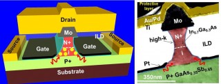
Schematic and cross-section transmission electron microscopy (TEM) image of a fabricated vertical Heterojunction Tunnel Field Effect Transistor (HTFET) |
Abstract:
Controlling power consumption in mobile devices and large scale data centers is a pressing concern for the computer chip industry. Researchers from Penn State and epitaxial wafer maker IQE have created a high performance transistor that could help solve one of the vexing problems of today's MOSFET technology - reducing the power demand whether the transistors are idle or switching.
Quantum Tunneling Results in Record Transistor Performance
University Park, PA | Posted on December 10th, 2011Today's digital information processing systems, from data centers to mobile laptops to smart phones, consume and dissipate significant power due to the constant power demand of the billions of transistors packed into the logic circuits on digital electronic devices. In traditional MOSFETs (metal-oxide semiconductor field-effect transistors), the building blocks of today's digital technology, a supply voltage of around one volt is required to gradually turn on the transistor. The current transistor technology faces inherent limits to reducing the power demand in electronic circuits due to physical laws related to the MOSFET design. Meanwhile, power demand will increase as the size of next generation transistors decreases and more devices are packed onto a computer chip.
In a paper to be delivered at the International Electron Devices Meeting in Washington DC on December 7th, Penn State doctoral candidate Dheeraj Mohata will discuss a new materials and device architecture that provides power savings and instant transistor on-off capability for future electronics. The paper, titled "Demonstration of MOSFET-Like On-Current Performance in Arsenide/Antimonide Tunnel FETs with Staggered Hetero-junctions for 300mV Logic Applications," reports the fabrication of a heterojunction field effect tunnel transistor with a 650% increase in drive current.
"This is the first time a tunneling field effect transistor has had a MOSFET-like On-state current," says Mohata's adviser Suman Datta, professor of electrical engineering. "By choosing two dissimilar semiconductor materials, Indium Gallium Arsenide and Gallium Arsenic Antimonide, and adjusting their composition, Deheeraj was able to engineer Hetero Tunnel FETs with a 7.6x improvement in drive current over the control sample." Tunneling FETs use the quantum mechanical property in which electrons are able to pass through a physical barrier if the barrier is thin enough. By increasing the drive current, the team was able to operate the Tunnel FET at reduced voltage, 300 milliVolt compared to 1V, thereby offering considerable power savings.
"If one can pick a proper combination of two different semiconductors and adjust their composition such that their band alignment results in a staggered configuration, it's possible to significantly increase the tunneling rate and enhance the drive current of the Tunnel FET," Datta explains.
The Penn State researchers designed and partnered with IQE, who produced the atomically precise multi-layer epiwafers using molecular beam epitaxy on which the transistors are built. The Penn State team then used advanced nanofabrication techniques to fabricate vertically oriented tunnel FET devices on the epiwafers in the Materials Research Institute's Nanofabrication Facility, whose director, professor of electrical engineering Theresa Mayer, was the co-principal investigator on the project. Comparing experimental results against the computer models used in the design phase enabled the researchers to verify their device simulations, and determine that Hetero Tunnel FETs would perform in a similar manner in the next generations of semiconductor devices, including future 7nm technology node devices.
"Work has to go on to see if this device can be further scaled to smaller dimensions and integrated on an industrial scale," Datta concludes. "If so, the impact will be significant in terms of low power integrated circuits that can work at 300 millivolts and below. This raises the possibility for self-powered circuits in conjunction with energy harvesting devices for active health monitoring, ambient intelligence, and implantable medical devices where the batteries haven't scaled in step with the devices."
Other members of the Penn State team along with Mohata, Datta, and Mayer include current and former graduate students, respectively, R. Bijesh and Salil Mujumdar in electrical engineering, graduate student Craig Eaton and assistant professor Roman Engel-Herbert in materials science and engineering, and Vijaykrishnan Narayanan, professor of computer engineering. Their research on Heterojunction Tunnel FETs was funded by Intel Corporation and the Nanoelectronics Research Institute (NRI)-supported Midwest Institute of Nanoelectronic Discovery (MIND). The Materials Research Institute's Nanofabrication Facility is a member of the National Nanofabrication Infrastructure Network (NNIN). Contact Suman Datta at .
The International Electron Devices Meeting (IEDM) is the world's premier forum for reporting breakthroughs in technology, design, manufacturing, physics, and the modeling of semiconductors and other electronic devices.
####
For more information, please click here
Contacts:
Suman Datta
Copyright © Newswise
If you have a comment, please Contact us.Issuers of news releases, not 7th Wave, Inc. or Nanotechnology Now, are solely responsible for the accuracy of the content.
Bookmark:


| Related News Press |
News and information
![]() Quantum computer improves AI predictions April 17th, 2026
Quantum computer improves AI predictions April 17th, 2026
![]() Flexible sensor gains sensitivity under pressure April 17th, 2026
Flexible sensor gains sensitivity under pressure April 17th, 2026
![]() A reusable chip for particulate matter sensing April 17th, 2026
A reusable chip for particulate matter sensing April 17th, 2026
![]() Detecting vibrational quantum beating in the predissociation dynamics of SF6 using time-resolved photoelectron spectroscopy April 17th, 2026
Detecting vibrational quantum beating in the predissociation dynamics of SF6 using time-resolved photoelectron spectroscopy April 17th, 2026
Chip Technology
![]() A reusable chip for particulate matter sensing April 17th, 2026
A reusable chip for particulate matter sensing April 17th, 2026
![]() Metasurfaces smooth light to boost magnetic sensing precision January 30th, 2026
Metasurfaces smooth light to boost magnetic sensing precision January 30th, 2026
Discoveries
![]() Quantum computer improves AI predictions April 17th, 2026
Quantum computer improves AI predictions April 17th, 2026
![]() Flexible sensor gains sensitivity under pressure April 17th, 2026
Flexible sensor gains sensitivity under pressure April 17th, 2026
![]() A reusable chip for particulate matter sensing April 17th, 2026
A reusable chip for particulate matter sensing April 17th, 2026
![]() Detecting vibrational quantum beating in the predissociation dynamics of SF6 using time-resolved photoelectron spectroscopy April 17th, 2026
Detecting vibrational quantum beating in the predissociation dynamics of SF6 using time-resolved photoelectron spectroscopy April 17th, 2026
Announcements
![]() A fundamentally new therapeutic approach to cystic fibrosis: Nanobody repairs cellular defect April 17th, 2026
A fundamentally new therapeutic approach to cystic fibrosis: Nanobody repairs cellular defect April 17th, 2026
![]() UC Irvine physicists discover method to reverse �quantum scrambling� : The work addresses the problem of information loss in quantum computing system April 17th, 2026
UC Irvine physicists discover method to reverse �quantum scrambling� : The work addresses the problem of information loss in quantum computing system April 17th, 2026
Events/Classes
![]() Institute for Nanoscience hosts annual proposal planning meeting May 16th, 2025
Institute for Nanoscience hosts annual proposal planning meeting May 16th, 2025
![]() A New Blue: Mysterious origin of the ribbontail ray�s electric blue spots revealed July 5th, 2024
A New Blue: Mysterious origin of the ribbontail ray�s electric blue spots revealed July 5th, 2024
![]() Researchers demonstrate co-propagation of quantum and classical signals: Study shows that quantum encryption can be implemented in existing fiber networks January 20th, 2023
Researchers demonstrate co-propagation of quantum and classical signals: Study shows that quantum encryption can be implemented in existing fiber networks January 20th, 2023
Quantum nanoscience
![]() Beyond silicon: Electronics at the scale of a single molecule January 30th, 2026
Beyond silicon: Electronics at the scale of a single molecule January 30th, 2026
![]() MXene nanomaterials enter a new dimension Multilayer nanomaterial: MXene flakes created at Drexel University show new promise as 1D scrolls January 30th, 2026
MXene nanomaterials enter a new dimension Multilayer nanomaterial: MXene flakes created at Drexel University show new promise as 1D scrolls January 30th, 2026
![]() ICFO researchers overcome long-standing bottleneck in single photon detection with twisted 2D materials August 8th, 2025
ICFO researchers overcome long-standing bottleneck in single photon detection with twisted 2D materials August 8th, 2025
|
|
||
|
|
||
| The latest news from around the world, FREE | ||
|
|
||
|
|
||
| Premium Products | ||
|
|
||
|
Only the news you want to read!
Learn More |
||
|
|
||
|
Full-service, expert consulting
Learn More |
||
|
|
||