Home > Press > Research: Graphene grows better on certain copper crystals
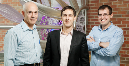 |
| Photo by L. Brian Stauffer
Professors Joseph Lyding, left, and Eric Pop, center, and graduate student Josh Wood identified copper crystal structures that work best for growing high-quality graphene. |
Abstract:
New observations could improve industrial production of high-quality graphene, hastening the era of graphene-based consumer electronics, thanks to University of Illinois engineers.
Research: Graphene grows better on certain copper crystals
Champaign, IL | Posted on October 28th, 2011By combining data from several imaging techniques, the team found that the quality of graphene depends on the crystal structure of the copper substrate it grows on. Led by electrical and computer engineering professors Joseph Lyding and Eric Pop, the researchers published their findings in the journal Nano Letters.
"Graphene is a very important material," Lyding said. "The future of electronics may depend on it. The quality of its production is one of the key unsolved problems in nanotechnology. This is a step in the direction of solving that problem."
To produce large sheets of graphene, methane gas is piped into a furnace containing a sheet of copper foil. When the methane strikes the copper, the
carbon-hydrogen bonds crack. Hydrogen escapes as gas, while the carbon sticks to the copper surface. The carbon atoms move around until they find each other and bond to make graphene. Copper is an appealing substrate because it is relatively cheap and promotes single-layer graphene growth, which is important for electronics applications.
"It's a very cost-effective, straightforward way to make graphene on a large scale," said Joshua Wood, a graduate student and the lead author of the paper.
"However, this does not take into consideration the subtleties of growing grapheme," he said. "Understanding these subtleties is important for making high-quality, high-performance electronics."
While graphene grown on copper tends to be better than graphene grown on other substrates, it remains riddled with defects and multi-layer sections, precluding high-performance applications. Researchers have speculated that the roughness of the copper surface may affect graphene growth, but the Illinois group found that the copper's crystal structure is more important.
Copper foils are a patchwork of different crystal structures. As the methane falls onto the foil surface, the shapes of the copper crystals it encounters affect how well the carbon atoms form graphene.
Different crystal shapes are assigned index numbers. Using several advanced imaging techniques, the Illinois team found that patches of copper with higher index numbers tend to have lower-quality graphene growth. They also found that two common crystal structures, numbered (100) and (111), have the worst and the best growth, respectively. The (100) crystals have a cubic shape, with wide gaps between atoms. Meanwhile, (111) has a densely packed hexagonal structure.
"In the (100) configuration the carbon atoms are more likely to stick in the holes in the copper on the atomic level, and then they stack vertically rather than diffusing out and growing laterally," Wood said. "The (111) surface is hexagonal, and graphene is also hexagonal. It's not to say there's a perfect match, but that there's a preferred match between the surfaces."
Researchers now are faced with balancing the cost of all (111) copper and the value of high-quality, defect-free graphene. It is possible to produce single-crystal copper, but it is difficult and prohibitively expensive.
The U. of I. team speculates that it may be possible to improve copper foil manufacturing so that it has a higher percentage of (111) crystals. Graphene grown on such foil would not be ideal, but may be "good enough" for most applications.
"The question is, how do you optimize it while still maintaining cost effectiveness for technological applications?" said Pop, a co-author of the paper. "As a community, we're still writing the cookbook for graphene. We're constantly refining our techniques, trying out new recipes. As with any technology in its infancy, we are still exploring what works and what doesn't."
Next, the researchers hope to use their methodology to study the growth of other two-dimensional materials, including insulators to improve graphene device performance. They also plan to follow up on their observations by growing graphene on single-crystal copper.
"There's a lot of confusion in the graphene business right now," Lyding said. "The fact that there is a clear observational difference between these different growth indices helps steer the research and will probably lead to more quantitative experiments as well as better modeling. This paper is funneling things in that direction."
Lyding and Pop are affiliated with the Beckman Institute for Advanced Science and Technology at the U. of I. The Office of Naval Research, the Air Force Office of Scientific Research, and the Army Research Office supported this research.
####
For more information, please click here
Contacts:
Liz Ahlberg
Physical Sciences Editor
217-244-1073
Joe Lyding
217-333-8370
Eric Pop
217-244-2070
Copyright © University of Illinois at Urbana-Champaign
If you have a comment, please Contact us.Issuers of news releases, not 7th Wave, Inc. or Nanotechnology Now, are solely responsible for the accuracy of the content.
Bookmark:


| Related Links |
| Related News Press |
News and information
![]() Quantum computer improves AI predictions April 17th, 2026
Quantum computer improves AI predictions April 17th, 2026
![]() Flexible sensor gains sensitivity under pressure April 17th, 2026
Flexible sensor gains sensitivity under pressure April 17th, 2026
![]() A reusable chip for particulate matter sensing April 17th, 2026
A reusable chip for particulate matter sensing April 17th, 2026
![]() Detecting vibrational quantum beating in the predissociation dynamics of SF6 using time-resolved photoelectron spectroscopy April 17th, 2026
Detecting vibrational quantum beating in the predissociation dynamics of SF6 using time-resolved photoelectron spectroscopy April 17th, 2026
Graphene/ Graphite
![]() Electrifying results shed light on graphene foam as a potential material for lab grown cartilage June 6th, 2025
Electrifying results shed light on graphene foam as a potential material for lab grown cartilage June 6th, 2025
![]() Breakthrough in proton barrier films using pore-free graphene oxide: Kumamoto University researchers achieve new milestone in advanced coating technologies September 13th, 2024
Breakthrough in proton barrier films using pore-free graphene oxide: Kumamoto University researchers achieve new milestone in advanced coating technologies September 13th, 2024
Govt.-Legislation/Regulation/Funding/Policy
![]() Quantum computer improves AI predictions April 17th, 2026
Quantum computer improves AI predictions April 17th, 2026
![]() Metasurfaces smooth light to boost magnetic sensing precision January 30th, 2026
Metasurfaces smooth light to boost magnetic sensing precision January 30th, 2026
![]() New imaging approach transforms study of bacterial biofilms August 8th, 2025
New imaging approach transforms study of bacterial biofilms August 8th, 2025
Chip Technology
![]() A reusable chip for particulate matter sensing April 17th, 2026
A reusable chip for particulate matter sensing April 17th, 2026
![]() Metasurfaces smooth light to boost magnetic sensing precision January 30th, 2026
Metasurfaces smooth light to boost magnetic sensing precision January 30th, 2026
Discoveries
![]() Quantum computer improves AI predictions April 17th, 2026
Quantum computer improves AI predictions April 17th, 2026
![]() Flexible sensor gains sensitivity under pressure April 17th, 2026
Flexible sensor gains sensitivity under pressure April 17th, 2026
![]() A reusable chip for particulate matter sensing April 17th, 2026
A reusable chip for particulate matter sensing April 17th, 2026
![]() Detecting vibrational quantum beating in the predissociation dynamics of SF6 using time-resolved photoelectron spectroscopy April 17th, 2026
Detecting vibrational quantum beating in the predissociation dynamics of SF6 using time-resolved photoelectron spectroscopy April 17th, 2026
Announcements
![]() A fundamentally new therapeutic approach to cystic fibrosis: Nanobody repairs cellular defect April 17th, 2026
A fundamentally new therapeutic approach to cystic fibrosis: Nanobody repairs cellular defect April 17th, 2026
![]() UC Irvine physicists discover method to reverse �quantum scrambling� : The work addresses the problem of information loss in quantum computing system April 17th, 2026
UC Irvine physicists discover method to reverse �quantum scrambling� : The work addresses the problem of information loss in quantum computing system April 17th, 2026
Military
![]() Quantum engineers �squeeze� laser frequency combs to make more sensitive gas sensors January 17th, 2025
Quantum engineers �squeeze� laser frequency combs to make more sensitive gas sensors January 17th, 2025
![]() Chainmail-like material could be the future of armor: First 2D mechanically interlocked polymer exhibits exceptional flexibility and strength January 17th, 2025
Chainmail-like material could be the future of armor: First 2D mechanically interlocked polymer exhibits exceptional flexibility and strength January 17th, 2025
![]() Single atoms show their true color July 5th, 2024
Single atoms show their true color July 5th, 2024
![]() NRL charters Navy�s quantum inertial navigation path to reduce drift April 5th, 2024
NRL charters Navy�s quantum inertial navigation path to reduce drift April 5th, 2024
|
|
||
|
|
||
| The latest news from around the world, FREE | ||
|
|
||
|
|
||
| Premium Products | ||
|
|
||
|
Only the news you want to read!
Learn More |
||
|
|
||
|
Full-service, expert consulting
Learn More |
||
|
|
||