Home > Press > Nanomaterials: Pillars of the assembly - Advanced electronics beckon thanks to self-assembling templates that allow the creation of nanoscale features on silicon wafers
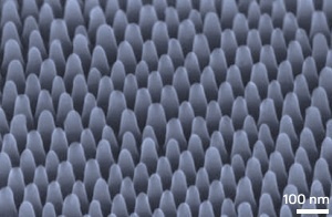 |
| Fine arrays of nanopillars can be patterned onto a silicon surface using a self-assembling polymer template Copyright : A*STAR |
Abstract:
The ever-increasing demand for enhanced performance in electronic devices such as solar cells, sensors and batteries is matched by a need to find ways to make smaller electrical components. Several techniques have been proposed for creating tiny, nanoscale structures on silicon, but these types of ‘nanopatterning' tend to involve low-throughput, high-cost approaches not suited to large-scale production. Sivashankar Krishnamoorthy and co-workers at the A*STAR Institute of Materials Research and Engineering have now found a simple and robust method for nanopatterning the entire surface of a silicon wafer.
Nanomaterials: Pillars of the assembly - Advanced electronics beckon thanks to self-assembling templates that allow the creation of nanoscale features on silicon wafers
Singapore | Posted on October 1st, 2011Krishnamoorthy's technique exploits the self-assembling properties of polymeric nanoparticles, known as reverse micelles. These unconventional particles have a structure consisting of a polar core and an outer layer of non-polar ‘arms'. Reverse micelles can form highly ordered arrays on the surface of a silicon wafer. The resulting ‘coating' can be used as a lithographic resist to mask the silicon surface during the etching process.
Although other groups have developed similar approaches in previous studies, Krishnamoorthy and co-workers are the first to develop a process that can pattern the entire surface of a silicon wafer with highly uniform nanostructures (see image). The authors have further developed a method to quantify nanostructure variations across large areas using simple optical tools, paving the way for high-throughput nanometrology.
In an additional improvement to the process, the researchers exposed the self-assembled polymer layer to a titanium chloride vapour. The titanium chloride selectively accumulates within each micelle's polar core. A blast of oxygen plasma then strips away the polymer to leave a pattern of tiny titanium oxide dots. This process converts a soft organic template into a hard inorganic mask much more suited to etching ultra-fine features into the silicon, producing arrays of nanopillars less than 10 nanometers apart.
The findings are expected to be highly adaptable. "Although we have demonstrated the process for creating silicon nanopillars, it is very versatile and can be readily extended to achieve nanopatterns of most other materials, for example, metals, semiconductors and polymers through appropriate post-processing of the initial copolymer templates," explains Krishnamoorthy. "Other patterns besides nanopillars could also be created, depending on the pattern-transfer processing employed."
Krishnamoorthy and his team are already exploring the potential applications of their technique. "We are currently making use of this process to create nanodevices for sensing, data storage, and energy applications, such as batteries and solar cells," Krishnamoorthy says.
The A*STAR-affiliated researchers contributing to this research are from the Institute of Materials Research and Engineering
References
Krishnamoorthy, S., Manipaddy, K. K., and Yap, F. L. Wafer-level self-organized copolymer templates for nanolithography with sub-50 nm feature and spatial resolutions. Advanced Functional Materials 21, 1102-1112 (2011).
####
For more information, please click here
Copyright © A*STAR Institute of Microelectronics (IME)
If you have a comment, please Contact us.Issuers of news releases, not 7th Wave, Inc. or Nanotechnology Now, are solely responsible for the accuracy of the content.
Bookmark:


| Related Links |
![]() Link to article on A*STAR research:
Link to article on A*STAR research:
![]() Institute of Materials Research and Engineering:
Institute of Materials Research and Engineering:
| Related News Press |
News and information
![]() Quantum computer improves AI predictions April 17th, 2026
Quantum computer improves AI predictions April 17th, 2026
![]() Flexible sensor gains sensitivity under pressure April 17th, 2026
Flexible sensor gains sensitivity under pressure April 17th, 2026
![]() A reusable chip for particulate matter sensing April 17th, 2026
A reusable chip for particulate matter sensing April 17th, 2026
![]() Detecting vibrational quantum beating in the predissociation dynamics of SF6 using time-resolved photoelectron spectroscopy April 17th, 2026
Detecting vibrational quantum beating in the predissociation dynamics of SF6 using time-resolved photoelectron spectroscopy April 17th, 2026
Chip Technology
![]() A reusable chip for particulate matter sensing April 17th, 2026
A reusable chip for particulate matter sensing April 17th, 2026
![]() Metasurfaces smooth light to boost magnetic sensing precision January 30th, 2026
Metasurfaces smooth light to boost magnetic sensing precision January 30th, 2026
Self Assembly
![]() Diamond glitter: A play of colors with artificial DNA crystals May 17th, 2024
Diamond glitter: A play of colors with artificial DNA crystals May 17th, 2024
![]() Liquid crystal templated chiral nanomaterials October 14th, 2022
Liquid crystal templated chiral nanomaterials October 14th, 2022
![]() Nanoclusters self-organize into centimeter-scale hierarchical assemblies April 22nd, 2022
Nanoclusters self-organize into centimeter-scale hierarchical assemblies April 22nd, 2022
![]() Atom by atom: building precise smaller nanoparticles with templates March 4th, 2022
Atom by atom: building precise smaller nanoparticles with templates March 4th, 2022
Nanoelectronics
![]() Lab to industry: InSe wafer-scale breakthrough for future electronics August 8th, 2025
Lab to industry: InSe wafer-scale breakthrough for future electronics August 8th, 2025
![]() Interdisciplinary: Rice team tackles the future of semiconductors Multiferroics could be the key to ultralow-energy computing October 6th, 2023
Interdisciplinary: Rice team tackles the future of semiconductors Multiferroics could be the key to ultralow-energy computing October 6th, 2023
![]() Key element for a scalable quantum computer: Physicists from Forschungszentrum Jülich and RWTH Aachen University demonstrate electron transport on a quantum chip September 23rd, 2022
Key element for a scalable quantum computer: Physicists from Forschungszentrum Jülich and RWTH Aachen University demonstrate electron transport on a quantum chip September 23rd, 2022
![]() Reduced power consumption in semiconductor devices September 23rd, 2022
Reduced power consumption in semiconductor devices September 23rd, 2022
Announcements
![]() A fundamentally new therapeutic approach to cystic fibrosis: Nanobody repairs cellular defect April 17th, 2026
A fundamentally new therapeutic approach to cystic fibrosis: Nanobody repairs cellular defect April 17th, 2026
![]() UC Irvine physicists discover method to reverse ‘quantum scrambling’ : The work addresses the problem of information loss in quantum computing system April 17th, 2026
UC Irvine physicists discover method to reverse ‘quantum scrambling’ : The work addresses the problem of information loss in quantum computing system April 17th, 2026
|
|
||
|
|
||
| The latest news from around the world, FREE | ||
|
|
||
|
|
||
| Premium Products | ||
|
|
||
|
Only the news you want to read!
Learn More |
||
|
|
||
|
Full-service, expert consulting
Learn More |
||
|
|
||