Home > Press > Building chips from collapsing nanopillars: By turning a common problem in chip manufacture into an advantage, MIT researchers produce structures only 30 atoms wide.
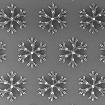 |
| Controlling the collapse of tiny pillars deposited on a silicon substrate can produce intricate patterns. |
Abstract:
The manufacture of nanoscale devices — the transistors in computer chips, the optics in communications chips, the mechanical systems in biosensors and in microfluidic and micromirror chips — still depends overwhelmingly on a technique known as photolithography. But ultimately, the size of the devices that photolithography can produce is limited by the very wavelength of light. As nanodevices get smaller, they'll demand new fabrication methods.
Building chips from collapsing nanopillars: By turning a common problem in chip manufacture into an advantage, MIT researchers produce structures only 30 atoms wide.
Cambridge, MA | Posted on September 1st, 2011In a pair of recent papers, researchers at MIT's Research Laboratory of Electronics and Singapore's Engineering Agency for Science, Technology and Research (A*STAR) have demonstrated a new technique that could produce chip features only 10 nanometers — or about 30 atoms — across. The researchers use existing methods to deposit narrow pillars of plastic on a chip's surface; then they cause the pillars to collapse in predetermined directions, covering the chip with intricate patterns.
Ironically, the work was an offshoot of research attempting to prevent the collapse of nanopillars. "Collapse of structures is one of the major problems that lithography down at the 10-nanometer level will face," says Karl Berggren, the Emanuel E. Landsman (1958) Associate Professor of Electrical Engineering and Computer Science, who led the new work. "Structurally, these things are not as rigid at that length scale. It's more like trying to get a hair to stand up. It just wants to flop over." Berggren and his colleagues were puzzling over the problem when, he says, it occurred to them that "if we can't end up beating it, maybe we can use it."
Status quo
With photolithography, chips are built up in layers, and after each layer is deposited, it's covered with a light-sensitive material called a resist. Light shining through an intricately patterned stencil — called a mask — exposes parts of the resist but not others, much the way light shining through a photographic negative exposes photo paper. The exposed parts of the resist harden, and the rest is removed. The part of the chip unprotected by the resist is then etched away, usually by an acid or plasma; the remaining resist is removed; and the whole process is repeated.
The size of the features etched into the chip is constrained, however, by the wavelength of light used, and chipmakers are already butting up against the limits of visible light. One possible alternative is using narrowly focused beams of electrons — or e-beams — to expose the resist. But e-beams don't expose the entire chip at once, the way light does; instead, they have to scan across the surface of the chip a row at a time. That makes e-beam lithography much less efficient than photolithography.
Etching a pillar into the resist, on the other hand, requires focusing an e-beam on only a single spot. Scattering sparse pillars across the chip and allowing them to collapse into more complex patterns could thus increase the efficiency of e-beam lithography.
The layer of resist deposited in e-beam lithography is so thin that, after the unexposed resist has been washed away, the fluid that naturally remains behind is enough to submerge the pillars. As the fluid evaporates and the pillars emerge, the surface tension of the fluid remaining between the pillars causes them to collapse.
Getting uneven
In the first of the two papers, published last year in the journal Nano Letters, Berggren and Huigao Duan, a visiting student from Lanzhou University in China, showed that when two pillars are very close to each other, they will collapse toward each other. In a follow-up paper, appearing in the Sept. 5 issue of the nanotech journal Small, Berggren, Duan (now at A*STAR) and Joel Yang (who did his PhD work with Berggren, also joining A*STAR after graduating in 2009) show that by controlling the shape of isolated pillars, they can get them to collapse in whatever direction they choose.
More particularly, slightly flattening one side of the pillar will cause it to collapse in the opposite direction. The researchers have no idea why, Berggren says: When they hatched the idea of asymmetric pillars, they expected them to collapse toward the flat side, the way a tree tends to collapse in the direction of the axe that's striking it. In experiments, the partially flattened pillars would collapse in the intended direction with about 98 percent reliability. "That's not acceptable from an industrial perspective," Berggren says, "but it's certainly fine as a starting point in an engineering demonstration."
At the moment, the technique does have its limitations. Space the pillars too close together, and they'll collapse toward each other, no matter their shape. That restricts the range of patterns that the technique can produce on chips with structures packed tightly together, as they are on computer chips.
But according to Joanna Aizenberg, the Amy Smith Berylson Professor of Materials Science at Harvard University, the applications where the technique will prove most useful may not have been imagined yet. "It can open the way to create structures that were just not possible before," Aizenberg says. "They're not in manufacturing yet because nobody knew how to make them."
Although Berggren and his colleagues didn't know it when they began their own experiments, for several years Aizenberg's group has been using the controlled collapse of structures on the micrometer scale to produce materials with novel optical properties. But "particularly interesting applications would come from this sub-100-nanometer scale," Aizenberg says. "It's a really amazing level of control of the nanostructure assembly that Karl's group has achieved."
####
For more information, please click here
Contacts:
77 Massachusetts Avenue, Room 11-400
Cambridge, MA 02139-4307
617.253.2700
TTY 617.258.9344
Copyright © MIT
If you have a comment, please Contact us.Issuers of news releases, not 7th Wave, Inc. or Nanotechnology Now, are solely responsible for the accuracy of the content.
Bookmark:


| Related News Press |
News and information
![]() Quantum computer improves AI predictions April 17th, 2026
Quantum computer improves AI predictions April 17th, 2026
![]() Flexible sensor gains sensitivity under pressure April 17th, 2026
Flexible sensor gains sensitivity under pressure April 17th, 2026
![]() A reusable chip for particulate matter sensing April 17th, 2026
A reusable chip for particulate matter sensing April 17th, 2026
![]() Detecting vibrational quantum beating in the predissociation dynamics of SF6 using time-resolved photoelectron spectroscopy April 17th, 2026
Detecting vibrational quantum beating in the predissociation dynamics of SF6 using time-resolved photoelectron spectroscopy April 17th, 2026
Microfluidics/Nanofluidics
![]() Projecting light to dispense liquids: A new route to ultra-precise microdroplets January 30th, 2026
Projecting light to dispense liquids: A new route to ultra-precise microdroplets January 30th, 2026
![]() Implantable device shrinks pancreatic tumors: Taming pancreatic cancer with intratumoral immunotherapy April 14th, 2023
Implantable device shrinks pancreatic tumors: Taming pancreatic cancer with intratumoral immunotherapy April 14th, 2023
![]() Researchers design new inks for 3D-printable wearable bioelectronics: Potential uses include printing electronic tattoos for medical tracking applications August 19th, 2022
Researchers design new inks for 3D-printable wearable bioelectronics: Potential uses include printing electronic tattoos for medical tracking applications August 19th, 2022
Chip Technology
![]() A reusable chip for particulate matter sensing April 17th, 2026
A reusable chip for particulate matter sensing April 17th, 2026
![]() Metasurfaces smooth light to boost magnetic sensing precision January 30th, 2026
Metasurfaces smooth light to boost magnetic sensing precision January 30th, 2026
Discoveries
![]() Quantum computer improves AI predictions April 17th, 2026
Quantum computer improves AI predictions April 17th, 2026
![]() Flexible sensor gains sensitivity under pressure April 17th, 2026
Flexible sensor gains sensitivity under pressure April 17th, 2026
![]() A reusable chip for particulate matter sensing April 17th, 2026
A reusable chip for particulate matter sensing April 17th, 2026
![]() Detecting vibrational quantum beating in the predissociation dynamics of SF6 using time-resolved photoelectron spectroscopy April 17th, 2026
Detecting vibrational quantum beating in the predissociation dynamics of SF6 using time-resolved photoelectron spectroscopy April 17th, 2026
Announcements
![]() A fundamentally new therapeutic approach to cystic fibrosis: Nanobody repairs cellular defect April 17th, 2026
A fundamentally new therapeutic approach to cystic fibrosis: Nanobody repairs cellular defect April 17th, 2026
![]() UC Irvine physicists discover method to reverse ‘quantum scrambling’ : The work addresses the problem of information loss in quantum computing system April 17th, 2026
UC Irvine physicists discover method to reverse ‘quantum scrambling’ : The work addresses the problem of information loss in quantum computing system April 17th, 2026
Photonics/Optics/Lasers
![]() Metasurfaces smooth light to boost magnetic sensing precision January 30th, 2026
Metasurfaces smooth light to boost magnetic sensing precision January 30th, 2026
![]() From sensors to smart systems: the rise of AI-driven photonic noses January 30th, 2026
From sensors to smart systems: the rise of AI-driven photonic noses January 30th, 2026
Printing/Lithography/Inkjet/Inks/Bio-printing/Dyes
![]() Presenting: Ultrasound-based printing of 3D materials—potentially inside the body December 8th, 2023
Presenting: Ultrasound-based printing of 3D materials—potentially inside the body December 8th, 2023
![]() Simple ballpoint pen can write custom LEDs August 11th, 2023
Simple ballpoint pen can write custom LEDs August 11th, 2023
![]() Disposable electronics on a simple sheet of paper October 7th, 2022
Disposable electronics on a simple sheet of paper October 7th, 2022
|
|
||
|
|
||
| The latest news from around the world, FREE | ||
|
|
||
|
|
||
| Premium Products | ||
|
|
||
|
Only the news you want to read!
Learn More |
||
|
|
||
|
Full-service, expert consulting
Learn More |
||
|
|
||