Home > Press > Two Graphene Layers May Be Better Than One
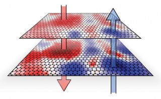 |
| NIST NIST measurements show that interactions of the graphene layers with the insulating substrate material causes electrons (red, down arrow) and electron holes (blue, up arrow) to collect in "puddles". The differing charge densities creates the random pattern of alternating dipoles and electron band gaps that vary across the layers. |
Abstract:
Researchers at the National Institute of Standards and Technology (NIST) have shown that the electronic properties of two layers of graphene vary on the nanometer scale. The surprising new results reveal that not only does the difference in the strength of the electric charges between the two layers vary across the layers, but they also actually reverse in sign to create randomly distributed puddles of alternating positive and negative charges. Reported in Nature Physics,* the new measurements bring graphene a step closer to being used in practical electronic devices.
Two Graphene Layers May Be Better Than One
Gaithersburg, MD | Posted on April 28th, 2011Graphene, a single layer of carbon atoms, is prized for its remarkable properties, not the least of which is the way it conducts electrons at high speed. However, the lack of what physicists call a band gap�an energetic threshold that makes it possible to turn a transistor on and off�makes graphene ill-suited for digital electronic applications.
Researchers have known that bilayer graphene, consisting of two stacked graphene layers, acts more like a semiconductor when immersed in an electric field.
According to NIST researcher Nikolai Zhitenev, the band gap may also form on its own due to variations in the sheets' electrical potential caused by interactions among the graphene electrons or with the substrate (usually a nonconducting, or insulating material) that the graphene is placed upon.
NIST fellow Joseph Stroscio says that their measurements indicate that interactions with the disordered insulating substrate material causes pools of electrons and electron holes (basically, the absence of electrons) to form in the graphene layers. Both electron and hole "pools" are deeper on the bottom layer because it is closer to the substrate. This difference in "pool" depths, or charge density, between the layers creates the random pattern of alternating charges and the spatially varying band gap.
Manipulating the purity of the substrate could give researchers a way to finely control graphene's band gap and may eventually lead to the fabrication of graphene-based transistors that can be turned on and off like a semiconductor.
Still, as shown in the group's previous work**, while these substrate interactions open the door to graphene's use as a practical electronic material, they lower the window on speed. Electrons do not move as well through substrate-mounted bilayer graphene; however, this may likely be compensated for by engineering the graphene/substrate interactions.
Stroscio's team plans to explore further the role that substrates may play in the creation and control of band gaps in graphene by using different substrate materials. If the substrate interactions can be reduced far enough, says Stroscio, the exotic quantum properties of bilayer graphene may be harnessed to create a new quantum field effect transistor.
* G. Rutter, S. Jung, N. Klimov, D. Newell, N. Zhitenev and J. Stroscio. Microscopic polarization in bilayer graphene. Nature Physics. Published online April 24, 2011.
####
For more information, please click here
Contacts:
Mark Esser
(301) 975-8735
Copyright © Newswise
If you have a comment, please Contact us.Issuers of news releases, not 7th Wave, Inc. or Nanotechnology Now, are solely responsible for the accuracy of the content.
Bookmark:


| Related Links |
![]() ** "See the Jan. 19, 2011, Tech Beat article "Real-World Graphene Devices May Have a Bumpy Ride" at:
** "See the Jan. 19, 2011, Tech Beat article "Real-World Graphene Devices May Have a Bumpy Ride" at:
| Related News Press |
News and information
![]() Quantum computer improves AI predictions April 17th, 2026
Quantum computer improves AI predictions April 17th, 2026
![]() Flexible sensor gains sensitivity under pressure April 17th, 2026
Flexible sensor gains sensitivity under pressure April 17th, 2026
![]() A reusable chip for particulate matter sensing April 17th, 2026
A reusable chip for particulate matter sensing April 17th, 2026
![]() Detecting vibrational quantum beating in the predissociation dynamics of SF6 using time-resolved photoelectron spectroscopy April 17th, 2026
Detecting vibrational quantum beating in the predissociation dynamics of SF6 using time-resolved photoelectron spectroscopy April 17th, 2026
Graphene/ Graphite
![]() Electrifying results shed light on graphene foam as a potential material for lab grown cartilage June 6th, 2025
Electrifying results shed light on graphene foam as a potential material for lab grown cartilage June 6th, 2025
![]() Breakthrough in proton barrier films using pore-free graphene oxide: Kumamoto University researchers achieve new milestone in advanced coating technologies September 13th, 2024
Breakthrough in proton barrier films using pore-free graphene oxide: Kumamoto University researchers achieve new milestone in advanced coating technologies September 13th, 2024
Govt.-Legislation/Regulation/Funding/Policy
![]() Quantum computer improves AI predictions April 17th, 2026
Quantum computer improves AI predictions April 17th, 2026
![]() Metasurfaces smooth light to boost magnetic sensing precision January 30th, 2026
Metasurfaces smooth light to boost magnetic sensing precision January 30th, 2026
![]() New imaging approach transforms study of bacterial biofilms August 8th, 2025
New imaging approach transforms study of bacterial biofilms August 8th, 2025
Chip Technology
![]() A reusable chip for particulate matter sensing April 17th, 2026
A reusable chip for particulate matter sensing April 17th, 2026
![]() Metasurfaces smooth light to boost magnetic sensing precision January 30th, 2026
Metasurfaces smooth light to boost magnetic sensing precision January 30th, 2026
Discoveries
![]() Quantum computer improves AI predictions April 17th, 2026
Quantum computer improves AI predictions April 17th, 2026
![]() Flexible sensor gains sensitivity under pressure April 17th, 2026
Flexible sensor gains sensitivity under pressure April 17th, 2026
![]() A reusable chip for particulate matter sensing April 17th, 2026
A reusable chip for particulate matter sensing April 17th, 2026
![]() Detecting vibrational quantum beating in the predissociation dynamics of SF6 using time-resolved photoelectron spectroscopy April 17th, 2026
Detecting vibrational quantum beating in the predissociation dynamics of SF6 using time-resolved photoelectron spectroscopy April 17th, 2026
Announcements
![]() A fundamentally new therapeutic approach to cystic fibrosis: Nanobody repairs cellular defect April 17th, 2026
A fundamentally new therapeutic approach to cystic fibrosis: Nanobody repairs cellular defect April 17th, 2026
![]() UC Irvine physicists discover method to reverse �quantum scrambling� : The work addresses the problem of information loss in quantum computing system April 17th, 2026
UC Irvine physicists discover method to reverse �quantum scrambling� : The work addresses the problem of information loss in quantum computing system April 17th, 2026
|
|
||
|
|
||
| The latest news from around the world, FREE | ||
|
|
||
|
|
||
| Premium Products | ||
|
|
||
|
Only the news you want to read!
Learn More |
||
|
|
||
|
Full-service, expert consulting
Learn More |
||
|
|
||