Home > Press > Boosting Memory Chips
 |
Abstract:
Moore's law predicts that the number of transistors on a silicon chip will double approximately every two years. Thanks to nano technology a similar acceleration is observed in data storage capability of memory chips
Boosting Memory Chips
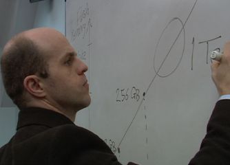
Italy | Posted on April 19th, 2011In each generation cycle memory chips get smaller and less expensive, but can hold more data. They are used in USB memory sticks, personal computers, video consoles and many other electronic devices. Further advances in electronics' technology rely now on the development of new materials and in particular on their manufacture in nano scale thin films. Atomic Layer Deposition (ALD) is a way to manufacture metal oxide materials layer by layer on the nano scale.
Within the EU research project REALISE synthetic chemists, materials scientists, electronic engineers and commercial project partners from all over Europe developed together an optimized process for nano scale deposition for the semiconductor manufacturing.
"Improvements in memory chips are now only possible by bringing in new materials that can be laid down with the high quality needed", says project coordinator Simon Elliott from Tyndall National Institute in Cork, Ireland.
The new materials are rare earth oxides: A fine powder that functions as an electronic insulator. It will isolate the electrical information on computer chips. The aim is to achieve a high dielectric material, with a so called high k-value, which would enable a large capacitance.
ASM Microchemistry in Helsinki, Finland, the chemical manufacturer partner in the project, has developed reactors that are able to deposit the rare earth oxides onto silicon wafers in a semi conductor line. The new process allows the scientists to put down these particular high-k dielectric films with a very high control and a very good quality and to do all that under clean room conditions.
Particle checks, electrical tests and measuring of the uniformity of the thickness have also been done with the processed wafers. The results are promising. All the elements are in place for the semi conductor industry to take on this new material when they are ready and produce the memory chip of the future.
####
For more information, please click here
Contacts:
Elisabeth Schmid
Phone: + 39 02 700 25 71
Fax: + 39 02 700 25 40
E-mail:
Copyright © youris.com
If you have a comment, please Contact us.Issuers of news releases, not 7th Wave, Inc. or Nanotechnology Now, are solely responsible for the accuracy of the content.
Bookmark:


| Related News Press |
News and information
![]() Quantum computer improves AI predictions April 17th, 2026
Quantum computer improves AI predictions April 17th, 2026
![]() Flexible sensor gains sensitivity under pressure April 17th, 2026
Flexible sensor gains sensitivity under pressure April 17th, 2026
![]() A reusable chip for particulate matter sensing April 17th, 2026
A reusable chip for particulate matter sensing April 17th, 2026
![]() Detecting vibrational quantum beating in the predissociation dynamics of SF6 using time-resolved photoelectron spectroscopy April 17th, 2026
Detecting vibrational quantum beating in the predissociation dynamics of SF6 using time-resolved photoelectron spectroscopy April 17th, 2026
Chip Technology
![]() A reusable chip for particulate matter sensing April 17th, 2026
A reusable chip for particulate matter sensing April 17th, 2026
![]() Metasurfaces smooth light to boost magnetic sensing precision January 30th, 2026
Metasurfaces smooth light to boost magnetic sensing precision January 30th, 2026
Memory Technology
![]() Researchers tackle the memory bottleneck stalling quantum computing October 3rd, 2025
Researchers tackle the memory bottleneck stalling quantum computing October 3rd, 2025
![]() First real-time observation of two-dimensional melting process: Researchers at Mainz University unveil new insights into magnetic vortex structures August 8th, 2025
First real-time observation of two-dimensional melting process: Researchers at Mainz University unveil new insights into magnetic vortex structures August 8th, 2025
![]() Utilizing palladium for addressing contact issues of buried oxide thin film transistors April 5th, 2024
Utilizing palladium for addressing contact issues of buried oxide thin film transistors April 5th, 2024
Announcements
![]() A fundamentally new therapeutic approach to cystic fibrosis: Nanobody repairs cellular defect April 17th, 2026
A fundamentally new therapeutic approach to cystic fibrosis: Nanobody repairs cellular defect April 17th, 2026
![]() UC Irvine physicists discover method to reverse �quantum scrambling� : The work addresses the problem of information loss in quantum computing system April 17th, 2026
UC Irvine physicists discover method to reverse �quantum scrambling� : The work addresses the problem of information loss in quantum computing system April 17th, 2026
Alliances/Trade associations/Partnerships/Distributorships
![]() Chicago Quantum Exchange welcomes six new partners highlighting quantum technology solutions, from Chicago and beyond September 23rd, 2022
Chicago Quantum Exchange welcomes six new partners highlighting quantum technology solutions, from Chicago and beyond September 23rd, 2022
![]() University of Illinois Chicago joins Brookhaven Lab's Quantum Center June 10th, 2022
University of Illinois Chicago joins Brookhaven Lab's Quantum Center June 10th, 2022
|
|
||
|
|
||
| The latest news from around the world, FREE | ||
|
|
||
|
|
||
| Premium Products | ||
|
|
||
|
Only the news you want to read!
Learn More |
||
|
|
||
|
Full-service, expert consulting
Learn More |
||
|
|
||