Home > Press > Templated growth technique produces graphene nanoribbons with metallic properties
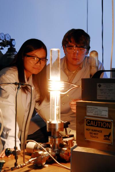 |
| Georgia Tech graduate students Yike Hu and John Hankinson observe a high-temperature furnace used to produce epitaxial graphene on a silicon carbide wafer. A new "templated growth" technique allows fabrication of nanoribbons with smooth edges and high conductivity.
Credit: Georgia Tech Photo: Gary Meek |
Abstract:
A new "templated growth" technique for fabricating nanoribbons of epitaxial graphene has produced structures just 15 to 40 nanometers wide that conduct current with almost no resistance. These structures could address the challenge of connecting graphene devices made with conventional architectures - and set the stage for a new generation of devices that take advantage of the quantum properties of electrons.
Templated growth technique produces graphene nanoribbons with metallic properties
Atlanta, GA | Posted on March 21st, 2011"We can now make very narrow, conductive nanoribbons that have quantum ballistic properties," said Walt de Heer, a professor in the School of Physics at the Georgia Institute of Technology. "These narrow ribbons become almost like a perfect metal. Electrons can move through them without scattering, just like they do in carbon nanotubes."
De Heer was scheduled to discuss recent results of this graphene growth process March 21st at the American Physical Society's March 2011 Meeting in Dallas. The research was sponsored by the National Science Foundation-supported Materials Research Science and Engineering Center (MRSEC).
First reported Oct. 3 in the advance online edition of the journal Nature Nanotechnology, the new fabrication technique allows production of epitaxial graphene structures with smooth edges. Earlier fabrication techniques that used electron beams to cut graphene sheets produced nanoribbon structures with rough edges that scattered electrons, causing interference. The resulting nanoribbons had properties more like insulators than conductors.
"In our templated growth approach, we have essentially eliminated the edges that take away from the desirable properties of graphene," de Heer explained. "The edges of the epitaxial graphene merge into the silicon carbide, producing properties that are really quite interesting."
The "templated growth" technique begins with etching patterns into the silicon carbide surfaces on which epitaxial graphene is grown. The patterns serve as templates directing the growth of graphene structures, allowing the formation of nanoribbons and other structures of specific widths and shapes without the use of cutting techniques that produce the rough edges.
In creating these graphene nanostructures, de Heer and his research team first use conventional microelectronics techniques to etch tiny "steps" - or contours - into a silicon carbide wafer whose surface has been made extremely flat. They then heat the contoured wafer to approximately 1,500 degrees Celsius, which initiates melting that polishes any rough edges left by the etching process.
Established techniques are then used for growing graphene from silicon carbide by driving off the silicon atoms from the surface. Instead of producing a consistent layer of graphene across the entire surface of the wafer, however, the researchers limit the heating time so that graphene grows only on portions of the contours.
The width of the resulting nanoribbons is proportional to the depth of the contours, providing a mechanism for precisely controlling the nanoribbon structures. To form complex structures, multiple etching steps can be carried out to create complex templates.
"This technique allows us to avoid the complicated e-beam lithography steps that people have been using to create structures in epitaxial graphene," de Heer noted. "We are seeing very good properties that show these structures can be used for real electronic applications."
Since publication of the Nature Nanotechnology paper, de Heer's team has been refining its technique. "We have taken this to an extreme - the cleanest and narrowest ribbons we can make," he said. "We expect to be able to do everything we need with the size ribbons that we are able to make right now, though we probably could reduce the width to 10 nanometers or less."
While the Georgia Tech team is continuing to develop high-frequency transistors - perhaps even at the terahertz range - its primary effort now focuses on developing quantum devices, de Heer said. Such devices were envisioned in the patents Georgia Tech holds on various epitaxial graphene processes.
"This means that the way we will be doing graphene electronics will be different," he explained. "We will not be following the model of using standard field-effect transistors (FETs), but will pursue devices that use ballistic conductors and quantum interference. We are headed straight into using the electron wave effects in graphene."
Taking advantage of the wave properties will allow electrons to be manipulated with techniques similar to those used by optical engineers. For instance, switching may be carried out using interference effects - separating beams of electrons and then recombining them in opposite phases to extinguish the signals.
Quantum devices would be smaller than conventional transistors and operate at lower power. Because of its ability to transport electrons with virtually no resistance, epitaxial graphene may be the ideal material for such devices, de Heer said.
"Using the quantum properties of electrons rather than the standard charged-particle properties means opening up new ways of looking at electronics," he predicted. "This is probably the way that electronics will evolve, and it appears that graphene is the ideal material for making this transition."
De Heer's research team hopes to demonstrate a rudimentary switch operating on the quantum interference principle within a year.
Epitaxial graphene may be the basis for a new generation of high-performance devices that will take advantage of the material's unique properties in applications where higher costs can be justified. Silicon, today's electronic material of choice, will continue to be used in applications where high-performance is not required, de Heer said.
"This is an important step in the process," he added. "There are going to be a lot of surprises as we move into these quantum devices and find out how they work. We have good reason to believe that this can be the basis for a new generation of transistors based on quantum interference."
####
For more information, please click here
Contacts:
John Toon
404-894-6986
Copyright © Georgia Institute of Technology
If you have a comment, please Contact us.Issuers of news releases, not 7th Wave, Inc. or Nanotechnology Now, are solely responsible for the accuracy of the content.
Bookmark:


| Related News Press |
News and information
![]() Quantum computer improves AI predictions April 17th, 2026
Quantum computer improves AI predictions April 17th, 2026
![]() Flexible sensor gains sensitivity under pressure April 17th, 2026
Flexible sensor gains sensitivity under pressure April 17th, 2026
![]() A reusable chip for particulate matter sensing April 17th, 2026
A reusable chip for particulate matter sensing April 17th, 2026
![]() Detecting vibrational quantum beating in the predissociation dynamics of SF6 using time-resolved photoelectron spectroscopy April 17th, 2026
Detecting vibrational quantum beating in the predissociation dynamics of SF6 using time-resolved photoelectron spectroscopy April 17th, 2026
Graphene/ Graphite
![]() Electrifying results shed light on graphene foam as a potential material for lab grown cartilage June 6th, 2025
Electrifying results shed light on graphene foam as a potential material for lab grown cartilage June 6th, 2025
![]() Breakthrough in proton barrier films using pore-free graphene oxide: Kumamoto University researchers achieve new milestone in advanced coating technologies September 13th, 2024
Breakthrough in proton barrier films using pore-free graphene oxide: Kumamoto University researchers achieve new milestone in advanced coating technologies September 13th, 2024
Chip Technology
![]() A reusable chip for particulate matter sensing April 17th, 2026
A reusable chip for particulate matter sensing April 17th, 2026
![]() Metasurfaces smooth light to boost magnetic sensing precision January 30th, 2026
Metasurfaces smooth light to boost magnetic sensing precision January 30th, 2026
Nanotubes/Buckyballs/Fullerenes/Nanorods/Nanostrings/Nanosheets
![]() Tiny nanosheets, big leap: A new sensor detects ethanol at ultra-low levels January 30th, 2026
Tiny nanosheets, big leap: A new sensor detects ethanol at ultra-low levels January 30th, 2026
![]() Enhancing power factor of p- and n-type single-walled carbon nanotubes April 25th, 2025
Enhancing power factor of p- and n-type single-walled carbon nanotubes April 25th, 2025
![]() Chainmail-like material could be the future of armor: First 2D mechanically interlocked polymer exhibits exceptional flexibility and strength January 17th, 2025
Chainmail-like material could be the future of armor: First 2D mechanically interlocked polymer exhibits exceptional flexibility and strength January 17th, 2025
![]() Innovative biomimetic superhydrophobic coating combines repair and buffering properties for superior anti-erosion December 13th, 2024
Innovative biomimetic superhydrophobic coating combines repair and buffering properties for superior anti-erosion December 13th, 2024
Discoveries
![]() Quantum computer improves AI predictions April 17th, 2026
Quantum computer improves AI predictions April 17th, 2026
![]() Flexible sensor gains sensitivity under pressure April 17th, 2026
Flexible sensor gains sensitivity under pressure April 17th, 2026
![]() A reusable chip for particulate matter sensing April 17th, 2026
A reusable chip for particulate matter sensing April 17th, 2026
![]() Detecting vibrational quantum beating in the predissociation dynamics of SF6 using time-resolved photoelectron spectroscopy April 17th, 2026
Detecting vibrational quantum beating in the predissociation dynamics of SF6 using time-resolved photoelectron spectroscopy April 17th, 2026
Announcements
![]() A fundamentally new therapeutic approach to cystic fibrosis: Nanobody repairs cellular defect April 17th, 2026
A fundamentally new therapeutic approach to cystic fibrosis: Nanobody repairs cellular defect April 17th, 2026
![]() UC Irvine physicists discover method to reverse �quantum scrambling� : The work addresses the problem of information loss in quantum computing system April 17th, 2026
UC Irvine physicists discover method to reverse �quantum scrambling� : The work addresses the problem of information loss in quantum computing system April 17th, 2026
Quantum nanoscience
![]() Beyond silicon: Electronics at the scale of a single molecule January 30th, 2026
Beyond silicon: Electronics at the scale of a single molecule January 30th, 2026
![]() MXene nanomaterials enter a new dimension Multilayer nanomaterial: MXene flakes created at Drexel University show new promise as 1D scrolls January 30th, 2026
MXene nanomaterials enter a new dimension Multilayer nanomaterial: MXene flakes created at Drexel University show new promise as 1D scrolls January 30th, 2026
![]() ICFO researchers overcome long-standing bottleneck in single photon detection with twisted 2D materials August 8th, 2025
ICFO researchers overcome long-standing bottleneck in single photon detection with twisted 2D materials August 8th, 2025
|
|
||
|
|
||
| The latest news from around the world, FREE | ||
|
|
||
|
|
||
| Premium Products | ||
|
|
||
|
Only the news you want to read!
Learn More |
||
|
|
||
|
Full-service, expert consulting
Learn More |
||
|
|
||