Home > Press > A Misunderstanding Leads to Method for Making Nanowells
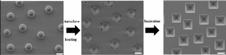 |
| Erik Hsiao Localized etching of a silicon (100) wafer upon hydrolysis of amidine-functionalized polystyrene latex colloids. The nanowell size can be precisely controlled with the size of the APSL colloids. No etch mask is needed and the region outside the nanowells is not etched at all. Scale Bar = 500 nm. |
Abstract:
A safe, simple, and cheap method of creating perfectly etched micron and smaller size wells in a variety of substrates has been developed by researchers in Penn State's Department of Chemical Engineering. Similar patterned surfaces are currently made using complex and expensive photolithography methods and etch processes under clean room conditions and used in the fabrication of many optical, electrical, and mechanical devices.
A Misunderstanding Leads to Method for Making Nanowells
University Park, PA | Posted on March 5th, 2011The nanowell discovery was made in the labs of Darrell Velegol and Seong Kim by Velegol's graduate student, Neetu Chaturvedi, and Kim's graduate student, Erik Hsiao. An article detailing their research, "Maskless Fabrication of Nanowells Using Chemically Reactive Colloids," appeared in the online edition of the journal Nano Letters in January 2011. In collaboration with Chaturvedi, Hsiao was working on a project to adhere polystyrene on a silicon wafer to create nanostructures with known dimensions. When Hsiao asked her to heat one of his samples, a miscommunication led her to heat the polystyrene and silicon wafer at low temperature in water in the autoclave normally used for biological samples rather than in the vacuum furnace. When they looked at the samples under the atomic force microscope (AFM), they noticed holes had formed beneath the polystyrene particles. Further examination under the scanning electron microscope (SEM) showed them perfectly etched, pyramidal shaped holes in the substrate below the places where the amidine-functionalized polystyrene latex colloid particles had adhered to the silicon dioxide on the surface of the silicon wafer.
"We saw three holes in the sample at the first AFM imaging and didn't know what it meant since we expected pancake-like polymer patches on the sample," said Hsiao. They took the sample to their advisers, who were both surprised by the etched wafer. By going over the steps the students had taken, the researchers realized that the wells were produced when the water hydrolized the amidine group in the particle, and through a series of chemical reactions, created a hydroxide ion that etched the well into the silicon wafer. The holes were uniform and their size and depth were totally dependent on the size of the original polystyrene particle, although the orientation of the silicon crystal affected the shape of the wells. In one orientation (100), the wells were perfect four-sided inverted pyramids. In the other orientation (111), the wells were perfect hexagons. The four researchers called them nanowells, because the bottom dimension of the wells was only a couple of nanometers across. They soon realized that they had discovered a new maskless method for creating structures in silicon without the elaborate steps normally required in the clean room.
"We're delivering hydroxide ions directly to where we want to etch," Velegol explained. "It's much safer and cheaper than electron beam and X-ray lithography. It's so safe that you could practically eat these particles without any harm."
"We think this is a quite general discovery," Kim added. "It's a way to deliver chemistry locally rather than in bulk. Many metals, ceramics, and other materials can be etched with this technique."
Another potential benefit of the discovery is the ability to create patterns on curved surfaces, something that is difficult to do with conventional photolithography. Since the particles are suspended in water, they can adhere to the surface of any shape and space themselves evenly over the surface. The researchers are just beginning to come up with intriguing ideas for how to use the simple technique.
Many breakthroughs come from accidents, Velegol remarked, because once something is known, people work on it very rapidly until they have filled in all the pieces and there is less to discover. Accidents are out of the pattern. "It's one of those situations like Pasteur said where chance favors the prepared mind. We would never even have thought to try this kind of chemistry. But Neetu had been working with these colloids for several years, and Erik had experience with the AFM, so they were well prepared to take advantage of the accident," Velegol concluded.
Neetu Chaturvedi, Ph.D., recently defended her thesis and is now a researcher with DuPont. Erik Hsiao is a graduate student in chemical engineering. Darrell Velegol is professor of chemical engineering and Seong Kim is associate professor of chemical engineering. Both are faculty in the Materials Research Institute where the AFM and SEM work was performed. Contact them by email at and This work was supported by the National Science Foundation (Grant Nos. IDR-1014673 and CMMI-1000021).
####
About Penn State Materials Research Institute
The Materials Research Institute facilitates and coordinates Penn State�s interdisciplinary research activity in materials science and engineering. The Millennium Science Complex, the university�s largest facility for scientific research, is scheduled to open in July 2011. It will bring together the Materials Research Institute and the Huck Institutes of the Life Sciences in the integration of the physical and life sciences with engineering.
For more information, please click here
Contacts:
Penn State Materials Research Institute
News office:
Pennsylvania State University
108 Materials Research Laboratory
University Park PA 16802
814-865-0285
Walter Mills
Associate Editor Publications
Materials Science
814-865-0285
Copyright © Penn State Materials Research Institute
If you have a comment, please Contact us.Issuers of news releases, not 7th Wave, Inc. or Nanotechnology Now, are solely responsible for the accuracy of the content.
Bookmark:


| Related News Press |
News and information
![]() Quantum computer improves AI predictions April 17th, 2026
Quantum computer improves AI predictions April 17th, 2026
![]() Flexible sensor gains sensitivity under pressure April 17th, 2026
Flexible sensor gains sensitivity under pressure April 17th, 2026
![]() A reusable chip for particulate matter sensing April 17th, 2026
A reusable chip for particulate matter sensing April 17th, 2026
![]() Detecting vibrational quantum beating in the predissociation dynamics of SF6 using time-resolved photoelectron spectroscopy April 17th, 2026
Detecting vibrational quantum beating in the predissociation dynamics of SF6 using time-resolved photoelectron spectroscopy April 17th, 2026
Govt.-Legislation/Regulation/Funding/Policy
![]() Quantum computer improves AI predictions April 17th, 2026
Quantum computer improves AI predictions April 17th, 2026
![]() Metasurfaces smooth light to boost magnetic sensing precision January 30th, 2026
Metasurfaces smooth light to boost magnetic sensing precision January 30th, 2026
![]() New imaging approach transforms study of bacterial biofilms August 8th, 2025
New imaging approach transforms study of bacterial biofilms August 8th, 2025
Chip Technology
![]() A reusable chip for particulate matter sensing April 17th, 2026
A reusable chip for particulate matter sensing April 17th, 2026
![]() Metasurfaces smooth light to boost magnetic sensing precision January 30th, 2026
Metasurfaces smooth light to boost magnetic sensing precision January 30th, 2026
Discoveries
![]() Quantum computer improves AI predictions April 17th, 2026
Quantum computer improves AI predictions April 17th, 2026
![]() Flexible sensor gains sensitivity under pressure April 17th, 2026
Flexible sensor gains sensitivity under pressure April 17th, 2026
![]() A reusable chip for particulate matter sensing April 17th, 2026
A reusable chip for particulate matter sensing April 17th, 2026
![]() Detecting vibrational quantum beating in the predissociation dynamics of SF6 using time-resolved photoelectron spectroscopy April 17th, 2026
Detecting vibrational quantum beating in the predissociation dynamics of SF6 using time-resolved photoelectron spectroscopy April 17th, 2026
Announcements
![]() A fundamentally new therapeutic approach to cystic fibrosis: Nanobody repairs cellular defect April 17th, 2026
A fundamentally new therapeutic approach to cystic fibrosis: Nanobody repairs cellular defect April 17th, 2026
![]() UC Irvine physicists discover method to reverse �quantum scrambling� : The work addresses the problem of information loss in quantum computing system April 17th, 2026
UC Irvine physicists discover method to reverse �quantum scrambling� : The work addresses the problem of information loss in quantum computing system April 17th, 2026
Grants/Sponsored Research/Awards/Scholarships/Gifts/Contests/Honors/Records
![]() Quantum computer improves AI predictions April 17th, 2026
Quantum computer improves AI predictions April 17th, 2026
![]() Detecting vibrational quantum beating in the predissociation dynamics of SF6 using time-resolved photoelectron spectroscopy April 17th, 2026
Detecting vibrational quantum beating in the predissociation dynamics of SF6 using time-resolved photoelectron spectroscopy April 17th, 2026
![]() Metasurfaces smooth light to boost magnetic sensing precision January 30th, 2026
Metasurfaces smooth light to boost magnetic sensing precision January 30th, 2026
|
|
||
|
|
||
| The latest news from around the world, FREE | ||
|
|
||
|
|
||
| Premium Products | ||
|
|
||
|
Only the news you want to read!
Learn More |
||
|
|
||
|
Full-service, expert consulting
Learn More |
||
|
|
||