Home > Press > WITec introduces “True Surface Microscopy”
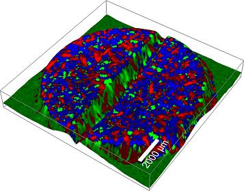 |
| An application example illustrating the working principle of True Surface Microscopy (Topographic Raman Image of a Pharmaceutical Tablet). |
Abstract:
Topographic Confocal Raman Imaging - The next evolutionary leap in cutting-edge microscope configurations
WITec introduces “True Surface Microscopy”
Ulm, Germany | Posted on December 8th, 2010WITec, worldwide leader in nano-analytical microscopy systems, has launched the new True Surface Microscopy option. The core element of this revolutionary imaging mode is an integrated sensor for optical profilometry. Large-area topographic coordinates from the profilometer measurement can be precisely correlated with the large-area confocal Raman imaging data. This allows for the first time confocal Raman imaging along heavily inclined or very rough samples with the true surface held in constant focus while maintaining the highest confocality. With the new imaging mode, samples that had previously required extensive preparation in order to obtain a certain surface flatness can now be effortlessly and automatically characterized as they are. Complete system control as well as extensive data evaluation are integrated within the WITec Control and WITec Project software environment, guaranteeing renowned ease-of-use.
"The integrated combination of optical profilometry and large-area confocal Raman imaging is the next evolutionary leap in cutting-edge microscope configurations." says Dr. Olaf Hollricher, WITec managing director R&D. "Only an inherently modular instrument design can enable such a seamless incorporation of a groundbreaking and complementary imaging technique into the present product line of Raman-AFM systems."
The profilometry capabilities of True Surface Imaging mode allows scan ranges of up to 100x100 mm with a spatial resolution on the order of 100 nm vertically and 10 µm laterally. Measuring distances of 10 mm and more provide flexibility for variable sample size requirements. In combination with AFM, the profilometer can even be used as a pre-inspection tool to determine topographic features of interest for high-resolution AFM investigations on large samples. The overall performance and exceptionally accurate imaging capabilities of True Surface Microscopy are beneficial for many applications, including the characterization of micromechanical, medical, or semiconductor devices, the mapping of functionalized surfaces, or the imaging of bio-medical or pharmaceutical material surface properties.
####
About WITec GmbH
WITec is a manufacturer of high performance optical and scanning probe microscopy systems. A modular product line allows the combination of different microscopy techniques such as Raman, SNOM or AFM in a single instrument for flexible analysis of the optical, chemical and structural properties of a sample. The instruments are distributed worldwide and are used primarily in the fields of Materials Science, Life Science and Nanotechnology. WITec is based in Ulm, Germany with regional headquarters in Maryville, TN, USA and Singapore.
For more information, please click here
Contacts:
Harald Fischer
Marketing Director
Tel: +49 (0) 731 140 70-0
Copyright © WITec GmbH
If you have a comment, please Contact us.Issuers of news releases, not 7th Wave, Inc. or Nanotechnology Now, are solely responsible for the accuracy of the content.
Bookmark:


| Related News Press |
News and information
![]() Quantum computer improves AI predictions April 17th, 2026
Quantum computer improves AI predictions April 17th, 2026
![]() Flexible sensor gains sensitivity under pressure April 17th, 2026
Flexible sensor gains sensitivity under pressure April 17th, 2026
![]() A reusable chip for particulate matter sensing April 17th, 2026
A reusable chip for particulate matter sensing April 17th, 2026
![]() Detecting vibrational quantum beating in the predissociation dynamics of SF6 using time-resolved photoelectron spectroscopy April 17th, 2026
Detecting vibrational quantum beating in the predissociation dynamics of SF6 using time-resolved photoelectron spectroscopy April 17th, 2026
Announcements
![]() A fundamentally new therapeutic approach to cystic fibrosis: Nanobody repairs cellular defect April 17th, 2026
A fundamentally new therapeutic approach to cystic fibrosis: Nanobody repairs cellular defect April 17th, 2026
![]() UC Irvine physicists discover method to reverse ‘quantum scrambling’ : The work addresses the problem of information loss in quantum computing system April 17th, 2026
UC Irvine physicists discover method to reverse ‘quantum scrambling’ : The work addresses the problem of information loss in quantum computing system April 17th, 2026
Tools
![]() Metasurfaces smooth light to boost magnetic sensing precision January 30th, 2026
Metasurfaces smooth light to boost magnetic sensing precision January 30th, 2026
![]() From sensors to smart systems: the rise of AI-driven photonic noses January 30th, 2026
From sensors to smart systems: the rise of AI-driven photonic noses January 30th, 2026
![]() Japan launches fully domestically produced quantum computer: Expo visitors to experience quantum computing firsthand August 8th, 2025
Japan launches fully domestically produced quantum computer: Expo visitors to experience quantum computing firsthand August 8th, 2025
|
|
||
|
|
||
| The latest news from around the world, FREE | ||
|
|
||
|
|
||
| Premium Products | ||
|
|
||
|
Only the news you want to read!
Learn More |
||
|
|
||
|
Full-service, expert consulting
Learn More |
||
|
|
||