Home > Press > Turning down the noise in graphene
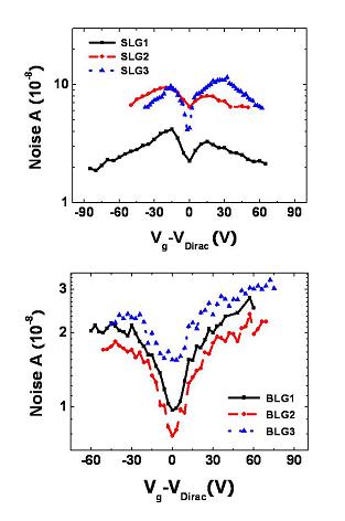 |
| New noise model shows all single layer graphene samples with an M-shaped pattern of noise (top) and all bi-layer graphene samples with a V-shaped noise pattern. |
Abstract:
Working with the unique nanoscience capabilities of the Molecular Foundry at the U.S. Department of Energy (DOE)'s Lawrence Berkeley National Laboratory, a multi-institutional team of researchers has developed the first model of signal-to-noise-ratios for low frequency noises in graphene on silica. Their results show noise patterns that run just the opposite of noise patterns in other electronic materials.
Turning down the noise in graphene
Berkeley, CA | Posted on August 7th, 2010Graphene is a two-dimensional crystalline sheet of carbon atoms - meaning it is only one atom thick - through which electrons can race at nearly the speed of light - 100 times faster than they can move through silicon. This plus graphene's incredible flexibility and mechanical strength make the material a potential superstar for the electronics industry. However, whereas the best electronic materials feature a strong signal and weak background noise, attaining this high signal-to-noise ratio has been a challenge for both single and bi-layers of graphene, especially when placed on a substrate of silica or some other dielectric. One of the problems facing device developers has been the lack of a good graphene noise model.
Working with the unique nanoscience capabilities of the Molecular Foundry at the U.S. Department of Energy (DOE)'s Lawrence Berkeley National Laboratory, a multi-institutional team of researchers has developed the first model of signal-to-noise-ratios for low frequency noises in graphene on silica. Their results show noise patterns that run just the opposite of noise patterns in other electronic materials.
Berkeley Lab materials scientist Yuegang Zhang led a study in which it was determined that for graphene on silica, the background signal noise is minimal near the region in the graphene where the electron density of states (the number of energy states available to each electron) is lowest. For semiconductors, such as silicon, in the region where electron density states is low the background noise is at its highest. However, there were distinct differences in the noise patterns of single and bi-layer graphene.
"In this work, we present the four-probe low frequency noise characteristics in single- and bi-layer graphene samples, using a back-gated device structure that helps simplify the physics in understanding the interactions between the graphene and the silica substrate," says Zhang. "For single-layer graphene we found that the noise was reduced either close to or far away from the lowest electron density of states, sometimes referred to as the Dirac point for graphene, forming an M-shaped pattern. For the bi-layer graphene, we found a similar noise reduction near the Dirac point but an increase away from that point, forming a V-shaped pattern. The noise data near the Dirac point correlated to spatial-charge inhomogeneity."
The results of this research are reported in the journal Nano Letters in a paper titled "Effect of Spatial Charge Inhomogeneity on 1/f Noise Behavior in Graphene." Co-authoring the paper with Zhang were Guangyu Xu, Carlos Torres Jr., Fei Liu, Emil Song, Minsheng Wang, Yi Zhou, Caifu Zeng and Kang Wang.
Lead author Guangyu Xu, a physicist with the Department of Electrical Engineering at the University of California (UC) Los Angeles, says the spatial charge inhomogeneity responsible for the graphene's unique noise patterns was probably caused by the charge impurities near the graphene-substrate interface.
"Our experiment carefully rules out other possible extrinsic factors that might influence the result," Xu says. "We conclude the correlation between the anomalous noise feature and the spatial charge inhomogeneity, is one of the main carrier scattering mechanisms for unsuspended graphene samples."
Xu says this model of low frequency noise characteristics in graphene should be a significant help for fabricating electronic devices because biasing at the low noise regime can be designed into the device.
"This will benefit the high signal-to-noise ratio in graphene," Xu says.
This work was supported in part by DOE's Office of Science.
The Molecular Foundry is one of the five DOE Nanoscale Science Research Centers (NSRCs), national user facilities for interdisciplinary research at the nanoscale, supported by the DOE Office of Science. Together the NSRCs comprise a suite of complementary facilities that provide researchers with state-of-the-art capabilities to fabricate, process, characterize and model nanoscale materials, and constitute the largest infrastructure investment of the National Nanotechnology Initiative. The other NSRCs are located at DOE's Argonne, Brookhaven, Oak Ridge and Sandia and Los Alamos National Laboratories.
####
About Berkeley Lab
Berkeley Lab is a U.S. Department of Energy (DOE) national laboratory located in Berkeley, California. It conducts unclassified scientific research and is managed by the University of California for the DOE Office of Science.
For more information, please click here
Contacts:
Lynn Yarris
(510) 486-5375
Copyright © Berkeley Lab
If you have a comment, please Contact us.Issuers of news releases, not 7th Wave, Inc. or Nanotechnology Now, are solely responsible for the accuracy of the content.
Bookmark:


| Related News Press |
News and information
![]() Quantum computer improves AI predictions April 17th, 2026
Quantum computer improves AI predictions April 17th, 2026
![]() Flexible sensor gains sensitivity under pressure April 17th, 2026
Flexible sensor gains sensitivity under pressure April 17th, 2026
![]() A reusable chip for particulate matter sensing April 17th, 2026
A reusable chip for particulate matter sensing April 17th, 2026
![]() Detecting vibrational quantum beating in the predissociation dynamics of SF6 using time-resolved photoelectron spectroscopy April 17th, 2026
Detecting vibrational quantum beating in the predissociation dynamics of SF6 using time-resolved photoelectron spectroscopy April 17th, 2026
Govt.-Legislation/Regulation/Funding/Policy
![]() Quantum computer improves AI predictions April 17th, 2026
Quantum computer improves AI predictions April 17th, 2026
![]() Metasurfaces smooth light to boost magnetic sensing precision January 30th, 2026
Metasurfaces smooth light to boost magnetic sensing precision January 30th, 2026
![]() New imaging approach transforms study of bacterial biofilms August 8th, 2025
New imaging approach transforms study of bacterial biofilms August 8th, 2025
Academic/Education
![]() Rice University launches Rice Synthetic Biology Institute to improve lives January 12th, 2024
Rice University launches Rice Synthetic Biology Institute to improve lives January 12th, 2024
![]() Multi-institution, $4.6 million NSF grant to fund nanotechnology training September 9th, 2022
Multi-institution, $4.6 million NSF grant to fund nanotechnology training September 9th, 2022
Nanotubes/Buckyballs/Fullerenes/Nanorods/Nanostrings/Nanosheets
![]() Tiny nanosheets, big leap: A new sensor detects ethanol at ultra-low levels January 30th, 2026
Tiny nanosheets, big leap: A new sensor detects ethanol at ultra-low levels January 30th, 2026
![]() Enhancing power factor of p- and n-type single-walled carbon nanotubes April 25th, 2025
Enhancing power factor of p- and n-type single-walled carbon nanotubes April 25th, 2025
![]() Chainmail-like material could be the future of armor: First 2D mechanically interlocked polymer exhibits exceptional flexibility and strength January 17th, 2025
Chainmail-like material could be the future of armor: First 2D mechanically interlocked polymer exhibits exceptional flexibility and strength January 17th, 2025
![]() Innovative biomimetic superhydrophobic coating combines repair and buffering properties for superior anti-erosion December 13th, 2024
Innovative biomimetic superhydrophobic coating combines repair and buffering properties for superior anti-erosion December 13th, 2024
Announcements
![]() A fundamentally new therapeutic approach to cystic fibrosis: Nanobody repairs cellular defect April 17th, 2026
A fundamentally new therapeutic approach to cystic fibrosis: Nanobody repairs cellular defect April 17th, 2026
![]() UC Irvine physicists discover method to reverse �quantum scrambling� : The work addresses the problem of information loss in quantum computing system April 17th, 2026
UC Irvine physicists discover method to reverse �quantum scrambling� : The work addresses the problem of information loss in quantum computing system April 17th, 2026
|
|
||
|
|
||
| The latest news from around the world, FREE | ||
|
|
||
|
|
||
| Premium Products | ||
|
|
||
|
Only the news you want to read!
Learn More |
||
|
|
||
|
Full-service, expert consulting
Learn More |
||
|
|
||